You are currently viewing SemiWiki as a guest which gives you limited access to the site. To view blog comments and experience other SemiWiki features you must be a registered member. Registration is fast, simple, and absolutely free so please,
join our community today!
WP_Term Object
(
    [term_id] => 157
    [name] => EDA
    [slug] => eda
    [term_group] => 0
    [term_taxonomy_id] => 157
    [taxonomy] => category
    [description] => Electronic Design Automation
    [parent] => 0
    [count] => 4441
    [filter] => raw
    [cat_ID] => 157
    [category_count] => 4441
    [category_description] => Electronic Design Automation
    [cat_name] => EDA
    [category_nicename] => eda
    [category_parent] => 0
    [is_post] =>
)
We have become accustomed to the idea that safety expectations can’t be narrowed down to one thing you do in design. They pervade all aspects of design from overall process through analysis, redundancies in design, fault analytics and mitigation for faults and on-board monitors for reliability among other requirements and techniques.… Read More
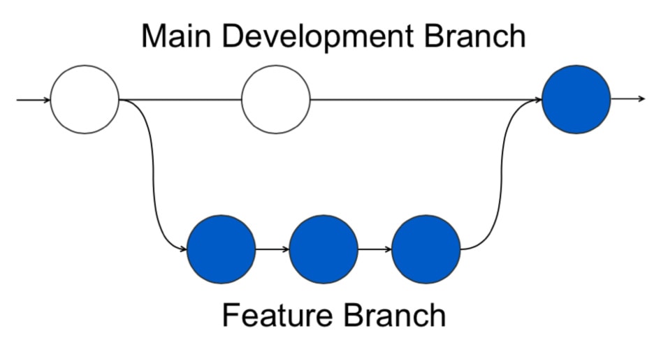
Linux creator Linus Torvalds lives in Oregon not too far from me and he also created the popular Git system for Design Management (DM) in 2004 that is now used by many software developers. So what makes Git so attractive as a DM tool?
- Feature-branch workflow
- Easy to switch context between features
- New features can be created orderly
…
Read More
Next week is SPIE, the leading lithography networking event here in Silicon Valley. Scott Jones is not only attending but also presenting at the 15th Annual LithoVision on Sunday. I will be at SPIE as well so if you want to meet up let us know. We will publish a blog on Scott’s presentation the morning of for those who cannot attend.… Read More
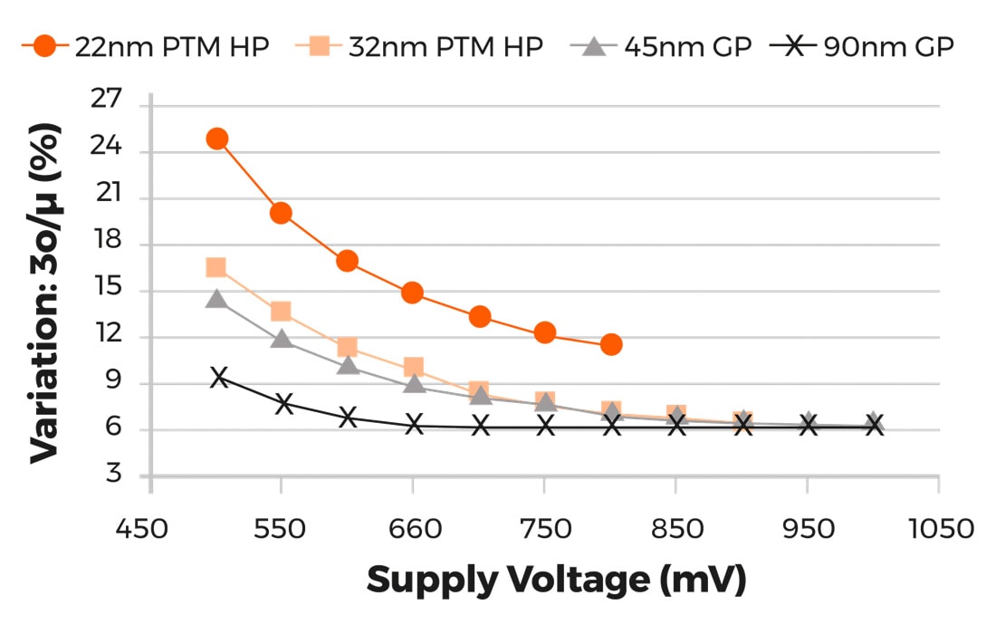
Variation analysis continues to be increasingly important as process technology moves to more advanced nodes. It comes as no surprise that tool development in this area has been vigorous and aggressive. New higher reliability IC applications, larger memory sizes and much higher production volumes require sophisticated yield… Read More
If you have a phone, you probably know it has a SIM card, for most of us the anchor that ties us into a 2/3-year plan with one network provider, unless you have an unlocked phone. Even then, you have to mess around swapping SIM cards if you travel overseas. Wouldn’t it be nice if the SIM was embedded and could be switched though an app or an… Read More
IPC-2581: The Standard for PCB Data Exchangeby Tom Dillinger on 02-19-2018 at 12:00 pmCategories: Cadence, EDA
The motivations to establish an industry standard data format are varied:
[LIST=1]
- solidify a “de facto” standard, transitioning its evolution and support from a single company to an industry consortium;
- aggregate disparate sources of design and manufacturing data into a single representation, with documented semantics;
…
Read More
DVCon turns 30 this year which is a very big deal. My oldest child also turns 30 this year which really puts things in perspective looking back at what we have all accomplished during that time. DVCon originally started as a user’s group at the 1988 Design Automation Conference in Anaheim California and the rest as they say is history.… Read More
At Intel back in the late 1970’s we wanted to know what process corner each DRAM chip and wafer was trending at so we included a handful of test transistors in the scribe lines between the active die. Having test transistors meant that we could do a quick electrical test at wafer probe time to measure the P and N channel transistor… Read More
Performance verification is among the most challenging of objectives in any SoC verification plan. It’s difficult to start effectively until quite late in the development cycle, at which point you don’t have a lot of time left to develop extensive performance-oriented testbenches. So many teams adapt functional tests to this… Read More
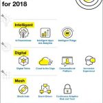
According to the Economist, “The world’s most valuable resource is no longer oil, but data”. Is this the case?Data is the by-product ofmany aspects of recent technology dynamics and is becoming the currency of today’s digital economy. All categories in Gartner’s Top10 Strategic Technology Trends for 2018 (Figure… Read More


Musk’s Orbital Compute Vision: TERAFAB and the End of the Terrestrial Data Center