You are currently viewing SemiWiki as a guest which gives you limited access to the site. To view blog comments and experience other SemiWiki features you must be a registered member. Registration is fast, simple, and absolutely free so please,
join our community today!
WP_Term Object
(
    [term_id] => 157
    [name] => EDA
    [slug] => eda
    [term_group] => 0
    [term_taxonomy_id] => 157
    [taxonomy] => category
    [description] => Electronic Design Automation
    [parent] => 0
    [count] => 4440
    [filter] => raw
    [cat_ID] => 157
    [category_count] => 4440
    [category_description] => Electronic Design Automation
    [cat_name] => EDA
    [category_nicename] => eda
    [category_parent] => 0
    [is_post] =>
)
I started out my engineering career by doing transistor-level circuit design and we used a proprietary SPICE circuit simulator. One thing that I quickly realized was that the accuracy of my circuit simulations depended entirely on the model files and parasitics. Here we are 40 years later and the accuracy of SPICE circuit simulations… Read More
During the 1940s when aerospace engineers were attempting to break the sound barrier for the first time, they were confronting a slew of new technical issues that had never been dealt with before, and in some cases never seen before. In subsonic flight airflow was predictable and well understood. In crossing the sound barrier, … Read More
The semiconductor conference season has started out strong and the premier verification gathering is coming up at the end of this month. SemiWiki bloggers, myself included, will be at the conference covering verification so you don’t have to. Verification is consuming more and more of the design cycle so I expect this event to … Read More
We have entered the age of AI specific processors, where specialized silicon is being produced to tackle the compute needs of AI. Whether they use GPUs, embedded programmable logic or specialized CPUs, many AI chips are based on parallel processing. This makes sense because of the parallel nature of AI computing. As a result, in… Read More
When floor planning (FP) and place & route (P&R) tools took over from custom layout tools for standard cell based designs, life became a lot better for designers of large digital chips. The beauty of the new flows was that all the internals of the standard cells and many IP blocks were hidden from view, lightening the load … Read More
The surge of network traffic at the data centers has driven to an increase in network bandwidth, doubling every 12-15 months according to a study conducted on Google’s data centers. The primary drivers to this uptick include the proliferation of cloud computing, more distributed storage architecture, emerging applications… Read More
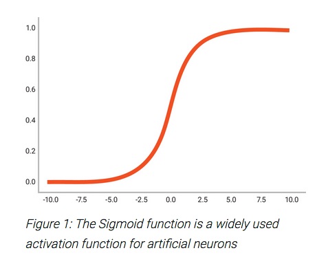
The field of artificial intelligence has relied on heavy inspiration from the world of natural intelligence, such as the human mind, to build working systems that can learn and act on new information based on that learning. In natural networks, neurons do the work, deciding when to fire based on huge numbers of inputs. The relationship… Read More
It is important when talking about a market to first establish the need and potential growth, then determine how the market is being served. This requires examining product features and services offered. … Read More
DesignCon is coming up, kicking off the first of many industry conferences for the year. It’s at the Santa Clara Convention Center which is the best venue in Northern California. Not only is this a semiconductor crowd, it’s also a systems crowd covering chips, boards, and systems. More than 175 companies participate with an expected… Read More
It seems that it has always been that there were packages and ICs, and in the design tool world “never the twain shall meet”. The tools for designing packages were completely separate from the tools used to design IC’s. This was so profoundly true that even after Cadence merged with Valid Logic back in the early 90’s, their Allegro … Read More


Musk’s Orbital Compute Vision: TERAFAB and the End of the Terrestrial Data Center