Rene Donkers, the company’s Co-founder and CEO, started his EDA career at Sagantec where he became responsible for world wide customer support and operations management. Ten years ago, Rene and a handful of people noticed a need in the design community for a standardized (portable) IP Validation approach to replace internal… Read More
Electronic Design Automation
Webinar: Optimize SoC Glitch Power with Accurate Analysis from RTL to Signoff
I had the opportunity to preview an upcoming webinar from Synopsys on SoC Glitch Power – what it is and how to reduce it. There is some eye-opening information in this webinar. Glitch power is a bigger problem than you may think and Synopsys has some excellent strategies to help reduce the problem. The webinar is available via replay… Read More
What’s At the Center of Your SoC Design Process?
I love starting a new project from scratch, because there’s that optimistic feeling of having no constraints and being able to creatively express myself and get the job done right this time. For SoC designs today there are teams of engineers and maybe a program manager plus a marketing person that define the features, budget… Read More
Synopsys Introduces Industry’s First Complete USB4 IP Solution
Synopsys announced an addition to its popular DesignWare IP portfolio recently that has some significant ramifications. The company announced the industry’s first complete USB4 IP solution. Before we get into the details of the announcement, let’s take a quick look at the USB standard and why it’s important.
Standards… Read More
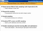
Webinar on Methods for Monte Carlo and High Sigma Analysis
There is an old saying popularized by Mark Twain that goes “There are three kinds of lies: lies, damned lies, and statistics.” It turns out that no one can say who originated this saying, yet despite however you might feel about statistics, they play an important role in verifying analog designs. The truth is that there are large numbers… Read More
Predicting Bugs: ML and Static Team Up. Innovation in Verification
Can we predict where bugs are most likely to be found, to better direct testing? Paul Cunningham (GM of Verification at Cadence), Jim Hogan and I continue our series on novel research ideas, again through a paper in software verification we find equally relevant to hardware. Feel free to comment if you agree or disagree.
The Innovation… Read More
WEBINAR: Adnan on Challenges in Security Verification
Adnan Hamid, CEO of Breker, has an interesting background. He was born in China to diplomat parents in the Bangladesh embassy. After I’m sure an equally interesting childhood, he got his BSEE/CS at Princeton. Where, like most of us he had to make money on the side, in his case working for a professor in the Psych lab on artificial intelligence… Read More
Do You Love DAC? Here’s Why I Do
Hello all, and welcome to DAC Season. As you all probably know by now, there are some twists to DAC Season this year. First, it’s being held July 20 – 24 this year instead of in June. I believe there was one other time the conference spilled into July, so this isn’t the norm. DAC, like pretty much every other conference these days has also… Read More
Automating the Analysis of Power MOSFET Designs
There’s a world of difference between our smart phones that are battery powered and pack billions of transistors, and power MOSFET devices that can be used in industrial applications, telecom, cloud computing and automotive where they could be run at a few hundred volts and up to 80A of current. I’ve read about one … Read More
Webinar Replay – Insight into Creating a Common Testbench
These days the verification process starts right when the design process begins, and it keeps going well past the end of the design phase. Simulation is used extensively at every stage of design and can go a long way to help validate a design. However, for many types of designs, especially those that process complex data streams, … Read More


Silicon Insurance: Why eFPGA is Cheaper Than a Respin — and Why It Matters in the Intel 18A Era