You are currently viewing SemiWiki as a guest which gives you limited access to the site. To view blog comments and experience other SemiWiki features you must be a registered member. Registration is fast, simple, and absolutely free so please,
join our community today!
WP_Term Object
(
    [term_id] => 96
    [name] => 5G
    [slug] => 5g
    [term_group] => 0
    [term_taxonomy_id] => 96
    [taxonomy] => category
    [description] =>
    [parent] => 0
    [count] => 113
    [filter] => raw
    [cat_ID] => 96
    [category_count] => 113
    [category_description] =>
    [cat_name] => 5G
    [category_nicename] => 5g
    [category_parent] => 0
    [is_post] =>
)
Physical AI is changing how intelligent systems interact with the real world. These systems must sense, process, and respond to data in real time. Unlike cloud AI, Physical AI depends on fast local processing and reliable distributed communication. This shift creates a new challenge. Systems must move large volumes of sensor… Read More
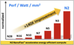
Intel’s historical dominance in semiconductor process technology began to erode around 2018, as competitors started delivering higher performance at smaller nodes. In response, Intel is now doubling down on innovation across two fronts: advanced process nodes such as Intel 18A and 14A, and cutting-edge packaging technologies.… Read More
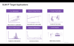
In an era defined by complex chip architectures, ever-shrinking technology nodes and very demanding applications, Silicon Lifecycle Management (SLM) has become a foundational strategy for optimizing performance, reliability, and efficiency across the lifespan of a semiconductor device. Central to effective SLM are Process,… Read More
Ceva recently unveiled its XC21 and XC23 DSP cores, designed to revolutionize wireless communications and edge AI processing. These new offerings build upon the Ceva-XC20 architecture, delivering unmatched efficiency, scalability, and performance for 5G-Advanced, pre-6G, and smart edge applications. As demand grows … Read More
Engineered substrate technology is driving an evolution within the semiconductor industry. As Moore’s Law reaches its limits, the focus is shifting from traditional planar wafer scaling to innovative material engineering and 3D integration. Companies like Soitec, Intel and Samsung are pioneering this transition, unlocking… Read More
The semiconductor industry continues to evolve rapidly to meet the escalating demands for speed, power efficiency, and miniaturization. As traditional silicon-based technologies reach their physical and performance limits, engineered substrates and advanced material innovation have emerged as pivotal drivers of the… Read More
There was a lot of discussion at IEDM about the coming shift to gate-all-around (GAA) transistor structures. This new device brings many benefits to continue device scaling, both at the monolithic device level as well as for multi-die design. The path to GAA is not simple, there are new material, process and design considerations… Read More
Prologue
Peter was running late for two reasons. First, he encountered unexpected heavy traffic and arrived ten minutes late for a crucial meeting with a customer to run a compliance test of his new 6G phone design prototyped on FPGAs. This prototype’s success was pivotal, as it could secure a significant purchase order.… Read More
In the fast-paced world of Electronic Design Automation (EDA), the complexity of chip designs is continuously rising. With the burgeoning of systems such as 5G communication devices and Advanced Driver-Assistance Systems (ADAS) teeming with thousands of components, the demand for robust and efficient prototyping platforms… Read More
I am a fan of product releases which bundle together multiple high-value advances. That approach reduces the frequency of releases (no bad thing) in exchange for more to offer per release, better proven through solid partner validation. The Dynamic Duo III release falls in this class, offering improvements in performance, capacity,… Read More


Musk’s Orbital Compute Vision: TERAFAB and the End of the Terrestrial Data Center