In the fabless world of semiconductor design, IP components have become indispensable partners and have enabled the development of complex billion gate SoCs. IP business in general is exhibiting a very high growth rate since couple of years and it is going to increase; the same is being reflected by a growing number of IP vendors… Read More
Author: Pawan Fangaria
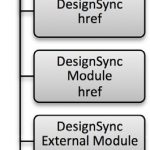
Flexible Integration System for IPs into SoC
The number of IPs with growing complexity and heterogeneity is ever increasing (counting into hundreds) to be integrated into a single SoC. It’s not possible to have them all available at once and in a single repository for the integration engineers to assemble all of them together and integrate into the SoC. The reality is that … Read More
LSI’s Way of Faster & Reliable Electronic System Design
LSI Corporationstarted in 1980s and I had several encounters with it during my jobs in 1990s; not to forget the LSI chips I used to see in desktops and other electronic systems, and I’m happy to see LSI continuing today with more vigour having leadership position in storage and networking space. It provides highly reliable, high … Read More
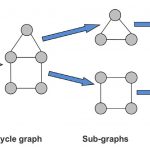
FinFET & Multi-patterning Need Special P&R Handling
I think by now a lot has been said about the necessity of multi-patterning at advanced technology nodes with extremely low feature size such as 20nm, because lithography using 193nm wavelength of light makes printing and manufacturing of semiconductor design very difficult. The multi-patterning is a novel semiconductor manufacturing… Read More
Secret of TI’s Success in Analog & Embedded Space
Since I started looking at the ways Texas Instrumentsworks through its strategies, my belief is getting firmed up that this is one company which can always sail through rough waters during downturn and reap rich benefits during upturn. They regularly review their strategies and can predict ahead of time when the water is about … Read More
Importance of Data Management in SoC Verification
In an era of SoCs with millions of gates, hundreds of IPs and multiple ways to verify designs through several stages of transformations at different levels of hierarchies, it is increasingly difficult to handle such large data in a consistent and efficient way. The hardware and software, and their interactions, have to be consistent… Read More
Ten Innovative Debugging Techniques – Pre & Post Layout
In a complex world of SoCs with multi-million gates and IPs from several heterogeneous sources, verification of a complete semiconductor design has become extremely difficult, and it’s not enough. In order to ascertain the right intent of the design throughout the design cycle, debugging at various stages of the design cycle… Read More
Signoff Accurate Timing Analysis at Improved Run-time & Capacity
The semiconductor design sizes, these days, can easily be of the order of several hundred millions of cells, adding into the complexity of verification. Amid ever growing design sizes, it’s a must that the timing verification is done accurately. Normally Static Timing Analysis (STA) is done to check whether all clocks and signals… Read More
Customization can add extraordinary power to your tool
In EDA arena we often find companies providing customization platforms along with the tools they offer to their customers. I admire such companies because they equip the end users of a tool to extend its functionality as they like according to their environment, thus increasing the designer productivity significantly. And I’m… Read More
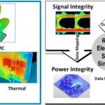
Fast & Accurate Thermal Analysis of 3D-ICs
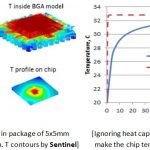
As Moore’s law started saturating on a single semiconductor die, the semiconductor community came up with the approach of growing vertically by stacking dies one above other in a 3D-IC arrangement. However, a major concern with a 3D-IC is that the heat generated by each die can get trapped in the stack, and hence it’s extremely important… Read More






Chemical Origins of Environmental Modifications to MOR Lithographic Chemistry