


What was the first EDA company name that came to your mind after reading that title?
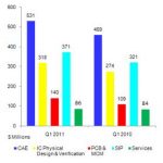
At Forbes magazine they rated both Mentor Graphics and Synopsys in the top 25 best companies for work life balance.
That’s quite an honor for both Mentor and Synopsys so I can say that EDA dominated the list this year.
Here are some of the factors… Read More


TSMC CoWoS versus Intel EMIB Semiconductor Packaging