You are currently viewing SemiWiki as a guest which gives you limited access to the site. To view blog comments and experience other SemiWiki features you must be a registered member. Registration is fast, simple, and absolutely free so please,
join our community today!
Right now I’m typing on my MacBook Pro computer connected to the Internet through WiFi, thanks to the electronics in both my laptop and WiFi router. I kind of take WiFi for granted because it is so ubiquitous throughout my daily life, yet there are IC designers at companies like Lantiq Semiconductorthat have to design and optimize… Read More
Digital designers are more numerous than analog IC designers, and so they tend to get more attention from EDA vendors in terms of tools and automation methodologies. For an analog design team with specialists focused separately on schematics and layout there are several methodology questions that need to be addressed, like:… Read More
We’ve blogged dozens of times about UVM– Universal Verification Methodology at SemiWiki, and all of the major EDA vendors support UVM, so you may be lulled into thinking that UVM is totally adequate for top-down SoC verification. Yesterday I had a phone discussion with Frank Schirrmeister of Cadence about a new approach… Read More
A recent comment by a DACattendee mentioned that the IoT acronym was so over-used as to make him get upset at EDA vendors that all purport to be enabling the growing IoT revolution. One of the most common requirements that I hear about IoT electronics is that the power needs to be well understood and controlled during the design exploration… Read More
Most IC designs are developed by a team of professionals, often separated into distinct groups like front-end and back-end, logical and physical designers. Circuit designers use tools like schematic capture at the transistor-level to create a topology, then begin simulating the netlist with a SPICE simulator. Layout designers… Read More
Software engineers and firmware designers can find bugs, update their code and re-distribute to the users. In the consumer electronics world this means that my smart phone apps get updated, and my Android OS gets updated on a somewhat regular basis, however on the hardware side the design and verification of an SoC must be close … Read More
I visited the Magwel booth at DAC in June and chatted with Dundar Dumlugol the CEO about their EDA tools that enable 3D co-simulation and extraction. Since then I’ve made contact with their CTO, Dr. Wim Schoenmaker to better understand what it’s like to start up and run an EDA company. Magwel’s history goes back… Read More
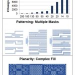
The traditional batch-oriented DRC process run as a final check to ensure compliance with foundry yield goals is quickly moving toward a concurrent DRC process performed early and often throughout design, especially at the 28 nm and smaller process nodes. What are the technology factors causing this change?
…
Read More
Last week I was traveling in Munich attending the MunEDA User Group meetingso I missed a live webinar on the topic of optimizing for power at RTL. I finally got caught up in my email this week and had time to view this 47 minute webinar, presented by Guillaume Boilletof Atrenta. He recommended using a combination of automatic, semi-automatic… Read More
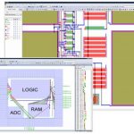
High-capacity IC place and route (P&R) tools can cost $200K and more to own from the big three vendors (Cadence, Synopsys, Mentor), but what about IC designs that are primarily Big Analog and Little Digital? In the EDA world we often have multiple choices for tools, and there are affordable alternatives to place and route out… Read More

















The Invisible Bottleneck Is Costing You Time You Can’t Get Back