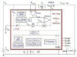
The Brazilian Ministry of Science and Technology (MCTIC) has a research unit, Renato Archer Information Technology Center (CTI), and two of their IC engineers presented at the MunEDA User Group meeting this May on the topic of designing Latching Current Limiter (LCL) circuits for space applications with RHBD (radiation-hardened… Read More
Author: Daniel Payne
Rad Hard Circuit Design and Optimization for Space Applications
RISC-V 64 bit IP for High Performance
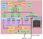
RISC-V as an Instruction Set Architecture (ISA) has grown quickly in commercial importance and relevance since its release to the open community in 2015, attracting many IP vendors that now provide a variety of RTL cores. Roger Espasa, CEO and Founder of Semidynamics, has presented at RISC-V events on how their IP is customized… Read More
Visit with Easy-Logic at #60DAC
I had read a little about Easy-Logic before #60DAC, so this meeting on Wednesday in Moscone West was my first in-person meeting with Jimmy Chen and Kager Tsai to learn about their EDA tools and where they fit into the overall IC design flow. A Functional Engineering Change Order (ECO) is a way to revise an IC design by updating the smallest… Read More
Empyrean visit at #60DAC
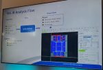
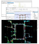
I arrived for my #60DAC booth appointment at Empyrean and was able to watch a customer presentation from Jason Guo, of Diodes. Jason was talking about how his company used the Patron tool for EM/IR analysis on their automotive chips. Diodes was found back in 1959 at Plano, Texas, and has since grown into 32 locations around the globe,… Read More
#60DAC Update from Arteris
I met up with Andy Nightingale, VP Product Marketing and Michal Siwinski, Chief Marketing Officer of Arteris at #60DAC for an update on their system IP company dealing with SoCs and chiplet-based designs. SemiWiki has been blogging about Arteris since 2011, and the company has grown enough in those 12 years to have an IPO, see their… Read More
Cadence and AI at #60DAC
Paul Cunningham from Cadence presented at the #60DAC Pavilion and gave one of the most optimistic visions of AI applied to EDA that I’ve witnessed, so hopefully I can convey some of his enthusiasm and outright excitement in my blog report. Mr. Cunningham reviewed the various ages of EDA design with each era providing about… Read More
Alphawave Semi Visit at #60DAC
On Wednesday at #60DAC I met Sudhir Mallya, Sr. VP Corporate Marketing at Alphawave Semi to get an update about what’s been happening at their IP company and with industry trends. The tagline for their company is: Accelerating the Connected World; and they have IP for connectivity, offer chiplet solutions, and even provide… Read More
Accellera and Clock Domain Crossing at #60DAC
Accellera sponsored a luncheon panel discussion at #60DAC, so I registered and attended to learn more about one of the newest working groups for Clock Domain Crossing (CDC). An overview of Accellera was provided by Lu Dai, then the panel discussion was moderated by Paul McLellan of Cadence, with the following panel members:
- Anupam
Agile Analog Visit at #60DAC
Chris Morrison, Director of Product Marketing at Agile Analog met with me on the Tuesday at DAC this year, and I asked what has changed in the last year for their analog IP business. The short answer is that the company has initially built up foundation IP for Analog Mixed-Signal (AMS) uses, then recently added new IP for data conversion,… Read More
Keysight EDA visit at #60DAC
The opening day at DAC was Monday and I had an appointment with Simon Rance (Cliosoft) and Stephen Slater, Product Manager of Keysight EDA in their suite. Back in February Daniel Nenni wrote about Keysight EDA acquiring Cliosoft, adding design data and IP management to their software offerings. I really wanted to hear how that … Read More







Captain America: Can Elon Musk Save America’s Chip Manufacturing Industry?