You are currently viewing SemiWiki as a guest which gives you limited access to the site. To view blog comments and experience other SemiWiki features you must be a registered member. Registration is fast, simple, and absolutely free so please,
join our community today!
While founder John Tanner, PhD, got his initial exposure to the TTL Cookbook and CMOS Cookbook as an undergraduate, it was his experience as a Caltech graduate student that forged his early path in EDA. In 1979, while enrolled in a VLSI design course at Caltech, John and his classmates received a pre-print of Carver Mead’s seminal… Read More
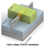
In my opinion, FinFETs will be the most significant piece of technology we, as semiconductor ecosystem people, will experience this decade. Seriously this is exciting stuff and one of the top search terms on SemiWiki for 6 months running. Here is a quick peek at what the top EDA companies will be talking about at the Common Platform… Read More
GLOBALFOUNDRIES changed the landscape of the foundry business in 2009 with a simple but ambitious plan to become the world’s first truly global foundry. At the Common Platform Technology Forum February 5th in the Santa Clara Convention Center GF Executive Vice President Michael Noonen will give an update on how that is … Read More
Sidense Corp. is a leading developer of embedded non-volatile memory (NVM) intellectual property (IP) for the semiconductor IC market. The company is headquartered in Ottawa, Canada, and has a global presence with sales offices worldwide.
The company was founded in 2004 by CTO Wlodek Kurjanowicz, a MoSys fellow and co-founder… Read More
In my never ending quest to promote the fabless semiconductor ecosystem I cannot pass up a discouraging word about one of the oldest financial services companies. You can consult with me for $300 per hour to answer your questions about the semiconductor industry on the phone or you can buy me lunch and get it in person (lunch will probably… Read More
Apache Design Solutions was founded in 2001 by Andrew Yang and three researchers from HP Labs (Norman Chang, Shen Lin, Weize Xie). They realized that engineers striving to meet the goal of increased device miniaturization, as defined by Moore’s Law, would eventually hit stumbling blocks in their progress. The founding team believed… Read More
Like any other event, the Consumer Electronics Show in Las Vegas is not immune to unethical and inappropriate behavior. Unfortunately one of digital media’s finest got caught this year doing what most publications have done since the beginning of time. CNET bowed to pressure from above and changed the outcome of the annual… Read More
If I had to describe CES in one word it would be exhausting. There were 3,000+ vendors, 150,000+ people, lines for everything, but 100% pure excitement. Even my beautiful wife was intrigued by the technology that shapes our lives. The smart toaster was of great interest to her since she says I time my toast with the smoke alarm. The … Read More
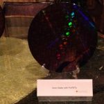
Incredibly exciting! Even my beautiful wife was impressed by the rainbow of colors it reflected. From left to right: 28nm, 20nm, and 14nm wafers. The 20nm and 14nm wafers are from the GLOBALFOUNDRIES NY fab, made in the USA! GF also announced another $3-4B CAPEX for 2013 to increase capacity of all three of their 300mm fabs (Singapore,… Read More
Let’s play word association. I say “EDA”, you immediately think “Synopsys”. I say “IP” and although 15 years ago you may not, today, you think “Synopsys”. For nearly two decades, Synopsys has grown its IP business through both organic development and acquisition, with a clear focus on enabling designers to meet their time-to-market… Read More


Captain America: Can Elon Musk Save America’s Chip Manufacturing Industry?