You are currently viewing SemiWiki as a guest which gives you limited access to the site. To view blog comments and experience other SemiWiki features you must be a registered member. Registration is fast, simple, and absolutely free so please,
join our community today!
There were two big announcements last week right in my backyard and I missed them both! Instead, I was in Taiwan investigating yet another big development and all three of these events will intersect next year, absolutely.
At IDF in San Francisco Intel outlined the new 14nm Core M. This is an impressive CPU, one that will fill the now… Read More
With four children entering the job market I have a very simple piece of advice: DO NOT RUN FROM TECHNOLOGY, EMBRACE IT! Smartphones are now a “natural” part of modern life. We work on them, we play on them, we shop with them, we socialize with them, even risk our lives using them. Come on, every single person with a smartphone has used… Read More
eSilicon, in conjunction with King Research, is conducting an unusual survey. A lot of vendor-driven surveys focus on specific pain points that are addressed by that particular vendor’s product/service. The idea is typically to either promote visibility for the product/service or establish its undeniable need in the market.… Read More
At the Citi Global Technology Conference last week Intel (INTC) CEO Brian Krzanich made some comments about the foundry business that I found quite misinformed. It will be interesting to see if this theme is repeated during the foundry presentations at the Intel Developer Forum in San Francisco this week:
Intel is presenting two… Read More
Intel (INTC) CEO Brian Krzanich keynoted the Citi Global Technology Conference last week. This was a precursor to the Intel Developer Forum in San Francisco this week. Normally these types of events are scripted dog and pony shows but sometimes interesting information comes out. The first question for example:
What does Intel… Read More
In looking at the SemiWiki analytics, one of the top search terms that brings traffic to our site is ARM, just about anything ARM. In fact, that’s what the next SemiWiki book will be about. Yes, ARM is that interesting. While EDA is also one of our top search terms, EDA+ARM will get the most views, absolutely. And let’s face it, bloggers… Read More
The nice thing about webinars is that if you register for the live one and you can’t attend you will still get first notice when the replay goes up. The other nice thing is that you can read a blog review of a webinar or whitepaper on SemiWiki first to see if it is worth your time. If you do attend a webinar you can also post a review of… Read More
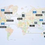
In the face of shrinking time-to-market windows, semiconductor companies are aggressively vying with each other to emerge with new or variants of existing ICs and SoCs to gain market share. The growth of the mobile market –wireless, networking, storage, and computing – as well as new areas such as the Internet of things (IoT) and… Read More
Raising four children is no easy task, believe me. My beautiful wife and I always felt it was important to foster the charitable side of our children by volunteering at the food bank, cleaning up local waterways, and other activities we could do as a family. To be clear, that is why my family did the ALS Ice Bucket Challenge.
“It is amazing… Read More
It looks like Sidense finally has closure on their request for attorney fees. Generally, in the U.S., parties in a lawsuit pay for their respective attorney fees which can be staggering. However, U.S. law allows the courts to shift the payment of the winner’s attorney fees to the losing party for “exceptional” reasons. Based on … Read More


Enhancing Multi-Domain System Simulation with FMI Co-Simulation