You are currently viewing SemiWiki as a guest which gives you limited access to the site. To view blog comments and experience other SemiWiki features you must be a registered member. Registration is fast, simple, and absolutely free so please,
join our community today!
The 2026 TSMC Open Innovation Platform (OIP) Ecosystem Forum was held on September 23, 2026, in Santa Clara, CA. This is the event where TSMC showcases the substantial progress made with its massive semiconductor ecosystem. As one would expect, AI was a key topic throughout the day, with some very impressive results reported and… Read More
About twenty years ago I worked with Cliff Hou, LC Lu, and the TSMC PDK team on reference flows with emerging EDA and IP companies. This was the precursor to the OIP. Having a person with LC Lu’s depth of R&D experience running the TSMC Design & Technology Platform is truly an honor, absolutely.
AI is creating two related… Read More
At the 2026 OIP Ecosystem Forum, the industry narrative shifted from incremental scaling to what TSMC defines as the “Intelligence Revolution.” Akin to the 18th-century Industrial Revolution which transitioned human physical labor to mechanical power, the current era is augmenting human ingenuity through … Read More
Daniel is joined by Aveek Sarkar, who heads TSMC’s Ecosystem and Alliance Management Division. Along with his team, he is responsible for driving semiconductor design enablement in collaboration with the partner ecosystem through TSMC’s Open Innovation Platform® (OIP). Prior to TSMC, Aveek worked on chip designs at Sun Microsystems… Read More
Chip-on-Wafer-on-Substrate, commonly called CoWoS, is an advanced packaging platform developed by TSMC. It allows processors, chiplets, and high-bandwidth memory stacks to be integrated within a single package. CoWoS has become especially important for artificial-intelligence accelerators and high-performance computing… Read More
TSMC reportedly plans to double its Chip-on-Wafer-on-Substrate capacity from approximately 130,000 300mm-equivalent wafers per month at the end of 2026 to 260,000 by 2028. The estimate is not formal company guidance and should be treated as a supply-chain projection. Nevertheless, the direction is consistent with TSMC’s… Read More
It’s that time of year again. Time certainly flies when AI is chasing you! This year marks the 18th TSMC OIP Ecosystem Forum, and it promises to be bigger and better than ever. My SemiWiki partners, Mike Gianfagna and Kalar Rajendiran, will join me in covering the event live, so stay tuned for all the news that’s fit to print.
Mike and… Read More
ASML and TSMC’s proposed shift from 6-inch to 12-inch photomasks is an attempt to redesign a critical but often overlooked part of advanced semiconductor manufacturing. Photomasks are precision plates carrying the circuit patterns projected by a lithography scanner onto a silicon wafer. In extreme-ultraviolet lithography,… Read More
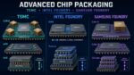
Advanced semiconductor packaging has become essential to improving computing performance as conventional transistor scaling grows more difficult and expensive. Instead of manufacturing an entire processor as one large monolithic die, chipmakers can divide it into smaller chiplets and combine logic, memory, input/output… Read More
TSMC’s overseas fabrication strategy is beginning to deliver its intended return: not immediate cost parity with Taiwan, but manufacturable geographic redundancy, closer integration with major customers and access to subsidized capacity in strategically important markets. Arizona and Kumamoto are already producing … Read More