Digital IC design has been largely automated with high-level languages, RTL coding, logic synthesis, and automated place and route tools. What about analog IC layout automation, is it possible? A few EDA companies think that it is possible and even practical. In recent memory there were two companies really focused on analog layout automation and that I also consulted for:
- Barcelona Design Automation, out of business in 2005
- Ciranova, acquired by Synopsys in 2012
Ed Petruswas VP of Engineering at Ciranova, however he moved over to Mentor Graphics in 2011 and his group just presented a paper at the 9th International Design and Test Symposium titled: Multi-Device Layout Templates for Nanometer Analog Design. This paper talks about a proposed EDA tool that automates the very difficult task of analog IC layout.
Related – Advances in Nanometer Analog and Mixed Signal Design!
Proper performance of many analog circuits requires that the transistors be matched in their physical layout. The goals of an automated tool would be:
- Generate complex analog layouts using Open Access (OA)
- Support commonly used analog circuits
- Use placement techniques like common centroid and stress avoidance
- Produce highly matched layouts
- Routing driven by user-constraints
- Free of DRC violations
- Support guard rings and dummy devices
Here’s the proposed tool flow for automating analog IC layout:
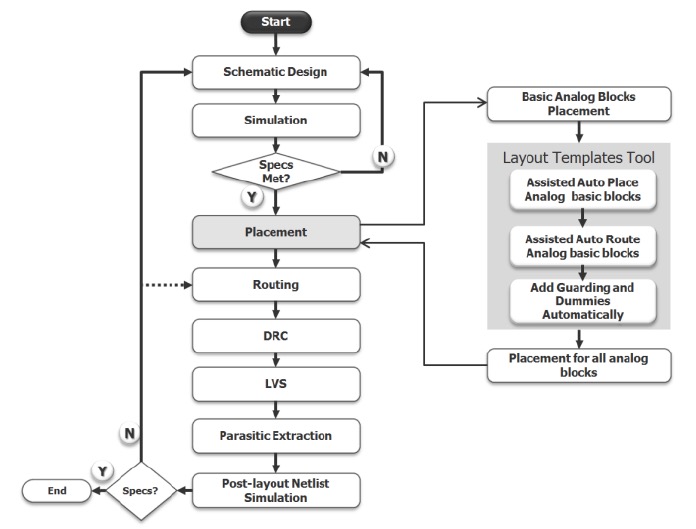
The Layout Templates Tool is where this methodology differs from manual placement and routing. The components of the Layout Templates Tool are shown below:
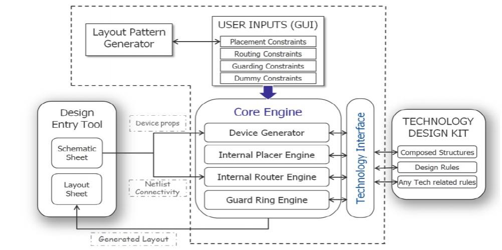
Using this approach you can generate an optimized layout for analog circuit topologies like: differential pairs, current mirrors and cascode current mirrors. A circuit designer uses schematic capture to select these devices and then defines the needed placement, routing, guard ring and dummy constraints through a GUI. The core engine accepts this info and automates the layout using device generators with technology from a design kit. There’s a layout pattern generator that has a set of pre-defined interdigitated patterns for each analog building block. Three placement methods are supported in the automatic pattern generator:
- Perfect Common Centroid (PCC)
- Common Centroid and Shallow Trench Isolation (CC&STI)
- Separate Placement (SP)
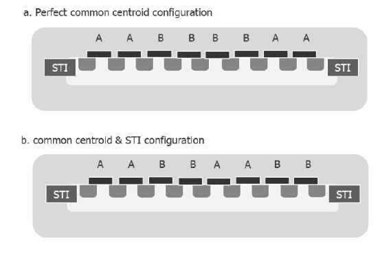
The internal placer engine uses a two-stage approach, device placement for a row followed by placement of rows. Internal routing also uses two stages, routing inside the row then routing between rows. Passive devices like capacitors can also be automated by using array placement.
Related – Full Spectrum Analog FastSPICE Useful for RF Designs on Bulk CMOS
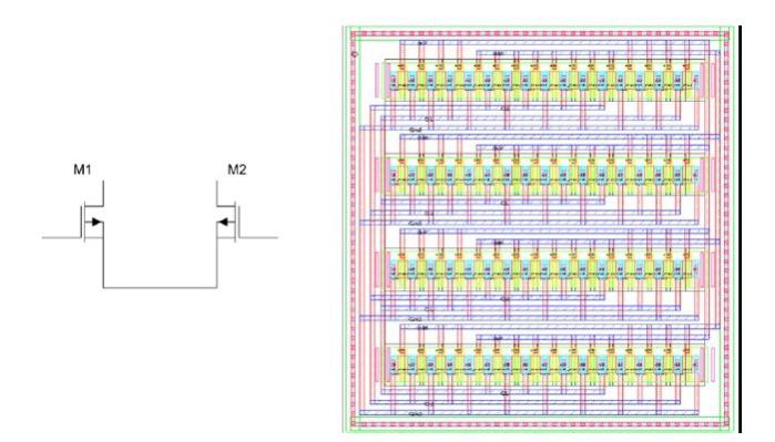
Here’s an example in 28 nm technology of a differential pair as a schematic and automated layout with interdigitation of PCC, without guard ring, and the number of finger/device = 32.
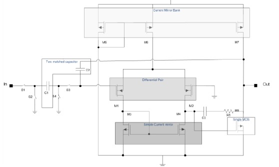
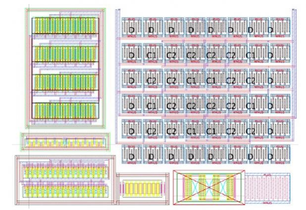
A more complex integrator circuit example has the following components:
- Differential pair
- Current mirror
- Current mirror bank
- Capacitor array
- MOS transistor
- Resistor
- Capacitor
Summary
Mentor Graphics has developed a capability to automate analog IC layout, so that the team of circuit designer and layout designer are more efficient, and spend less time doing manual chores, less time running DRC checks, and less time iterating to meet specifications. I look forward to a formal product announcement in the future. The complete 6 page conference paper is available here.
Share this post via:


Comments
0 Replies to “Can You Really Automate Analog IC Layout?”
You must register or log in to view/post comments.