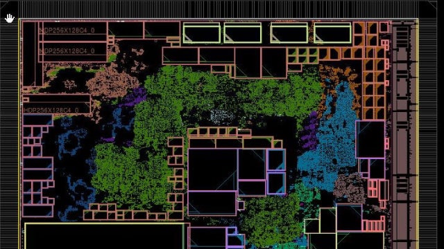
Automatic Place and Route (APR) tools have been around since the 1980s for IC design teams to use, and before that routing was done manually by very patient layout designers. Initially the big IDMs had their own internal CAD groups coding APR tools in house, but eventually the commercial EDA market picked up this automation area, and it’s been a highly competitive segment ever since then. Users of APR tools have a few metrics that they follow closely:
- Capacity, # of cells in a block
- Runtime
- Quality of Results, did I meet area, timing and power goals?
- Memory usage
- Number of DRC violations to fix after APR
I just had a video call with Henry Chang at Siemens EDA about their latest APR tool release of Aprisa 21.R1, and it was an eye opener. On capacity, he mentioned that many users run blocks in Aprisa that are 3-4 million instances, although some teams prefer to run larger blocks with 8-9 million instances. The tool can be run in either flat or hierarchical mode, and the big news is that on the largest designs the run times are up to 2X faster than the previous release. So, how did they do that?

You may recall that Siemens EDA acquired Avatar last year, July 2020. The engineers working on the previous routing tool Nitro combined to work on Aprisa, and then management hired even more developers to get the runtime improvements, so developer headcount increased by more than 2X. Not only did the runtime improve by an average of 30% for all designs, but the RAM usage decreased by up to 60% as well. Most APR jobs are run locally on a big server, so being more efficient is attractive to engineering departments., especially when their biggest jobs can run for a few days.
Aprisa developers improved pretty much all parts of the tool:
- Placement optimization
- Clock Tree Synthesis (CTS) optimization
- Route optimization
- Timing analysis
APR, like most critical EDA tools goes through a qualification process at the foundries, and Aprisa is fully certified for the TSMC 6nm process, while the 5nm and 4nm nodes have implemented all of the required design rules and features, so stay tuned for the official announcement of qualifications for these nodes.
Modern SoCs often use multi-power domains (MPD), and Aprisa handles that too. It sounds like the QoR with Aprisa come about in part by their approach to detailed routing, and there’s a previous blog on that topic.
Henry Chang
I first met Henry at Mentor Graphics, back in 2000, when we worked on a Fast-SPICE circuit simulator called Mach TA. He started his EDA career in 1993 as a co-founder and architect at Anagram, and had stints at Avant! and Atoptech, so he really understands the IC design process from SPICE to AMS and APR.
Summary
APR tool users have choices when it comes to finding and using a leading-edge tool for design implementation, and having a multi-vendor tool flow is a solid choice. Siemens EDA has bulked up their Aprisa team, and the improvements that are now revealed in faster run times, with a smaller memory footprint look impressive, with foundry support qualified at 6nm, and a pipeline to include 5nm and 4nm nodes well underway. Read the press release online.
Related Blogs
- Siemens EDA wants to help you engineer a smarter future faster
- Update on Mentor’s Acquisition of Avatar Integrated Systems
- Detail-Route-Centric Physical Implementation for 7nm
- Apogee Pipelining in Real Time
- Aprisa and Apogee – The New Avatars
- ATopTech is Back!
Share this post via:


Comments
There are no comments yet.
You must register or log in to view/post comments.