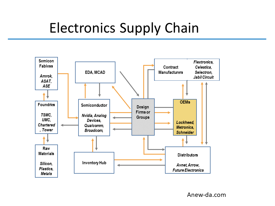
Since the formation of the Electronic Design Automation (EDA) industry in the 1970s, Moore’s law has increased functionality onto a semiconductor die dramatically. In response, EDA tools for semiconductor design have also grown in functionality and the design processes for semiconductors have moved forward at a breakneck pace. Interestingly, during the same timeframe, board design has largely stayed stagnant. Many of the major platforms for PCB design are decades old with specific additions in areas such as high-speed interconnect and advanced packaging.
Observation one: For the vast majority of system designers, PCB design today is not too dissimilar from the design process from the 1980s.
Further, there is a large and growing chasm for system designers between consumer and non-consumer products. Consumer markets drive the level of volume which is very interesting for semiconductor companies. To support the consumer markets, semiconductor companies provide focused application resources and in some rare cases will even build custom silicon for the system provider. However, the vast majority of system designers in very important markets (energy, defense, aerospace, and industrial) face an environment which is still dominated by the age old manual datasheet. The only real computer aid is the PDF textual search. Beyond the data sheet, the various important EDA artifacts of the chip such as mechanical structure, pinout, software drivers are disaggregated across vendors (often connected to EDA tool libraries) and must be chased down. Overall, it is a very manual, tedious, and error prone process.

The major players in the semiconductor ecosystem (figure above) certainly have a desire to help their customers, and there is an attempt to help system level designers with various capabilities. These include:
- Reference Designs: Semiconductor vendors publish reference designs on their websites focused on communicating the proper way to use their chips.
- Application Notes: Semiconductor and other players often write application notes which discuss the applicability of electronics systems in particular vertical markets.
Observation 2: There is a sea of information available on the internet, but it is distributed on a variety of websites in various non-standard ways. The only real automation mechanism available to a system designer is google search. However, a generic textual search engine has its limitations in a semantically rich environment such as electronics system design.
Aggregators such as distributors certainly have made an effort to service system designers in the part selection process. Vendors such as Digikey and Mouser provide some insights on the availability of parts based on high level selection of hardware functionality on their websites.
Observation 3: The part selection process is focused on semiconductor chips, so it does not provide clarity on the ability of other methods of implementing the same function. These might include sub functions in larger SoCs, programmable fabrics, software emulation, and more. This is simply not the focus of distributors today.
In fact, the fundamental design factors for most system designers such as operating environment, the vertical market certifications, important ecosystems (ARM, x86, etc), and useful lifetime of product are not addressed in any existing EDA system today. This leaves designers with the unenviable task of wading gingerly into an ocean of disorganized information. Further, semiconductor chip design has a deep capability which defines and enforces design rules through the implementation of automated checks by EDA tools. This ranges from layout DRC to logical assertions. PCB design systems certainly have some concept of layout DRC, but the higher levels of checks surrounding logical connections do not exist in the system board design suite.
Overall, the lack of automation at the system design level has an impact on designer productivity as well as correctness, and this is becoming an increasing problem. Why?
AI/IOT mega-trend: As “The Coming Evolution in Electronics Design Automation” describes, the next big mega-trend is the move of electronics to the edge with sensor, analog, DSP, and cloud connected systems. A key enablement of this paradigm is a highly productive design capability.
The millennial designer: While datasheets may be the preferred method of communication for seasoned designers, the newer generation of designers expect a much higher degree of automation.
In conclusion, with the current productivity of the system design process, the limiting factor for semiconductor growth in non-consumer markets will increasingly become designer bandwidth. Much like semiconductor EDA, there is a need to invest in system design EDA capability to unleash the power of electronics to solve important societal problems in fields ranging from defense to sustainability.
Also Read:
The Coming Evolution in Electronics Design Automation
The Increasing Gaps in PLM Systems with Handling Electronics
The Increasing Gap between Semiconductor Companies and their Customers
Share this post via:


Intel’s Path to Technological Leadership: Transforming Foundry Services and Embracing AI