
At the AI Infra Summit 2025, Synopsys showed how artificial intelligence has become inseparable from the process of creating advanced silicon. The company’s message was clear: AI is an end-to-end engine that drives every phase of chip development. Three Synopsys leaders illustrated this from distinct vantage points. Godwin Maben, Synopsys Fellow, delivered a talk on designing ultra–energy-efficient AI chips. Arun Venkatachar, Vice President of AI & Central Engineering, joined a dynamic panel on the impact of AI on semiconductor startups. And Frank Schirrmeister, Executive Director of Strategic Programs, gave a talk on meeting the quadrillion-cycle verification demands of modern datacenter designs. Together, their sessions formed a comprehensive narrative of how Synopsys enables greener, faster, and more reliable silicon.
Designing for Energy Efficiency
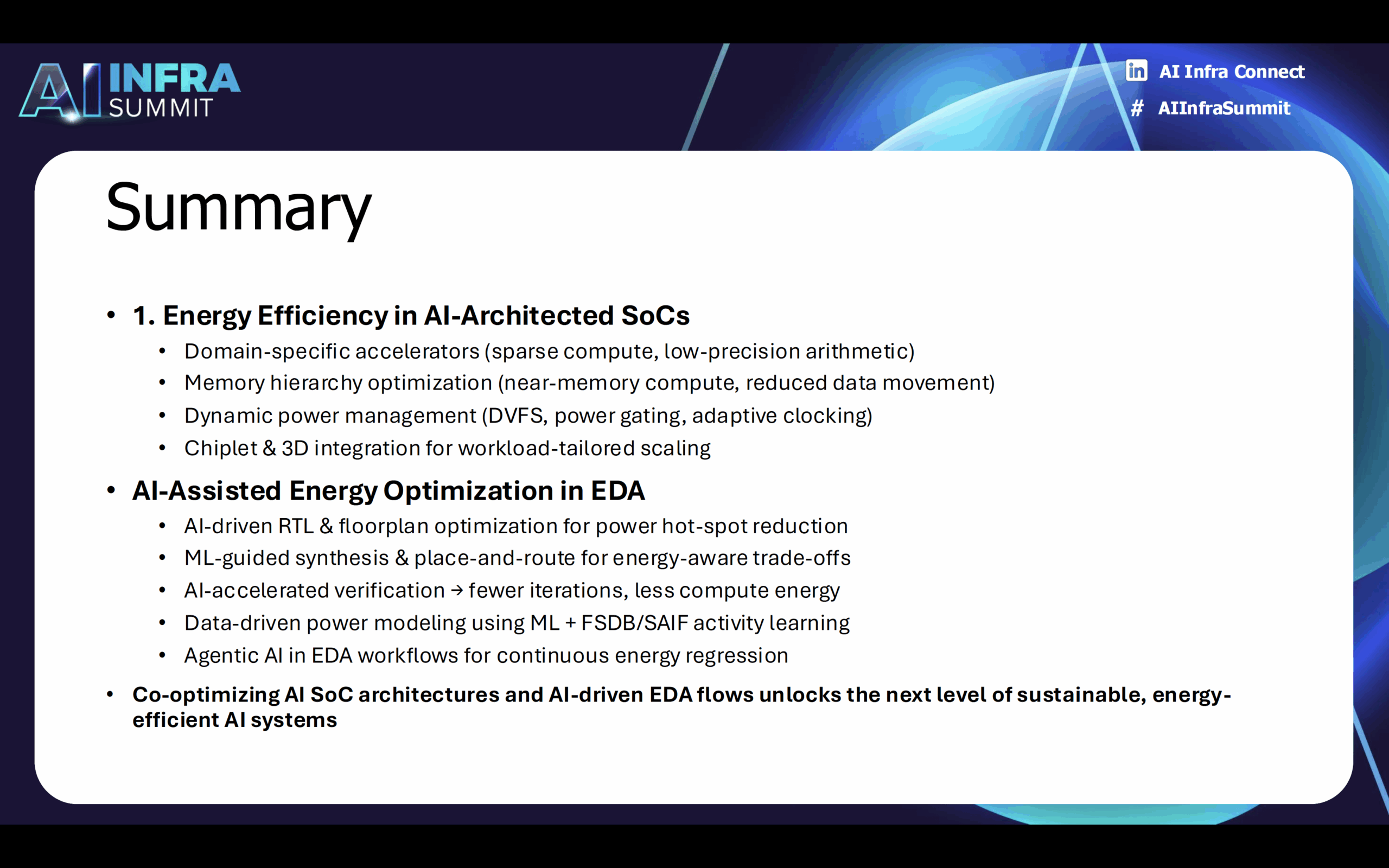
Godwin set the context with a stark statistic: AI workloads are projected to grow fifty-fold by 2028, threatening to overwhelm datacenter power budgets. He described how next-generation system-on-chip (SoC) designs must balance unprecedented performance with aggressive energy targets. Domain-specific accelerators, near-memory compute, and chiplet-based 3D integration all play a role, but Godwin emphasized that the real breakthrough comes when AI-driven electronic design automation (EDA) is applied at every level. Machine-learning-guided synthesis, floor-plan optimization, and continuous energy regression allow architects to reduce power per watt while meeting tight performance and area goals. His talk highlighted that sustainable AI silicon isn’t a final step—it’s architected in from the start.

Accelerating the Design Flow
In the panel session “The Impact of AI on Semiconductor Startups,” Arun explained how Synopsys began weaving machine learning into its design tools nearly a decade ago, well before today’s hype cycle. That early start is paying off. AI now informs power, performance, and area (PPA) optimization, verification, and manufacturing test, enabling some customers to cut design times by as much as 40 percent. Arun stressed that this isn’t about replacing engineers; rather, AI acts as a force multiplier, automating routine tasks and surfacing optimal design choices so human experts can focus on system-level creativity. He painted a picture of a continuous AI-assisted pipeline where improvements in one stage cascade into the next, shortening schedules and reducing the risk of late-stage surprises. For startups, this means faster paths to market and the ability to compete with established players.
Arun also discussed how cloud-based EDA is enabling startups to accelerate time to results and drive improvements by leveraging scalable, AI-powered development tools that empower small teams to achieve breakthrough innovation more efficiently.
Verifying at Quadrillion-Cycle Scale
Frank turned the spotlight on the most daunting phase: verification. Modern datacenter chips integrate multi-die architectures, Arm-based compute subsystems, and heterogeneous accelerators. Ensuring these complex systems meet power, performance, and reliability targets requires quadrillions of verification cycles. Traditional simulation alone can’t keep pace. Frank outlined how Synopsys addresses the challenge with hardware-assisted verification (HAV), including ZeBu emulation, HAPS prototyping, and EP-Ready hardware that seamlessly switches between emulation and prototyping. These platforms support early software bring-up, high-fidelity power analysis, and rapid coverage closure, allowing design teams to meet yearly product refresh cycles without compromising quality or budget.

Customer proof points from companies like Microsoft, NVIDIA, and AMD underscore the productivity gains.

A Unified AI-Driven Pipeline
What emerges from these three perspectives is a powerful theme: AI is now the connective fabric of the semiconductor lifecycle. Godwin’s focus on energy efficiency, Arun’s account of AI-assisted design flows, and Frank’s hardware-accelerated verification all reveal different facets of the same strategy. Synopsys doesn’t merely provide point tools; it delivers a continuous, AI-enabled ecosystem that shortens time-to-market, minimizes energy consumption, and raises confidence in first-silicon success.
The Summit sessions also highlighted Synopsys’s broader collaborations—with cloud providers for scalable compute, with Arm for ready-to-integrate IP, and with hyperscalers eager to validate enormous AI workloads. These partnerships reinforce the company’s role as the hub where cutting-edge design, advanced verification, and manufacturing readiness converge.
Summary
AI Infra Summit 2025 confirmed that designing the next generation of silicon is no longer about isolated breakthroughs. It is about orchestrating every step—architecture, layout, verification, and manufacturing—as one AI-driven continuum. Synopsys has been preparing for this moment for years, and the results are clear: faster design cycles, lower power footprints, and reliable chips that scale from edge devices to the largest datacenters.
By bringing together energy-efficient architecture, accelerated design flows, and quadrillion-cycle verification under a single AI umbrella, Synopsys demonstrated that “AI everywhere in the chip lifecycle” is the roadmap for the future of semiconductor innovation.
Also Read:
Synopsys Announces Expanding AI Capabilities and EDA AI Leadership
The Rise, Fall, and Rebirth of In-Circuit Emulation (Part 1 of 2)
eBook on Mastering AI Chip Complexity: Pathways to First-Pass Silicon Success
Share this post via:


Comments
There are no comments yet.
You must register or log in to view/post comments.