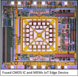
In my 34 years in IC and EDA, it never ceases to amaze me as to how ingenious designers can be with what is given them. Mentor, a Siemens business, has released a wonderful white paper that is proof of this yet again. The white paper steps through how one of their customers, MEMSIC, used the Tanner tool suite to develop a combination CMOS IC and MEMs accelerometer on a single die with no moving parts. This IC is truly intriguing and ingenious. It’s a mixture of digital, analog, and MEMs that uses heated gas molecules to sense 3-axis accelerations. More on this in a second…
The other thing that I found interesting in this white paper is that it gives a quick, succinct overview of how one goes about merging these multiple domains together on a single die. Many people now routinely mix analog and digital on an IC, but adding the MEMs part is tricky. The secret sauce is to have a design flow that enables the designer to plug the foreign entity (the MEMs in this case) into a standard analog/mixed signal design flow. The second and third parts of the solution are to then have a way to efficiently do the layout and modeling of the MEMs components and then bring the model back into the overall system simulation with digital, analog and MEMs. The Mentor Tanner solution tool does all that.
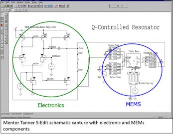
The first part is simple enough. Add a set of symbols into the schematic capture library and a set of pcells into the layout library that enable the capture and layout of both the electrical and the MEMs components. In addition, you also need models for all the components (electrical and mechanical). Electrical models already exist in your foundry PDK. The MEMs models must be created from scratch. In this flow, designers can either use analytical equations that can be directly simulated in spice or they can code the MEMs behavior in Verilog-A. OK, so far, that’s straight forward, assuming you know the analytical equations for your MEMs components.
The second part is doing the layout for the MEMs and then third part is back annotating a more accurate model of the MEMs for re-simulation. The second step is usually where designers mess up. The problem is that most MEMs designers are used to designing MEMs and not electronics. As such they typically start with a 3D-mesh model of their layout that they iterate through a series of finite element analysis (FEA) simulations to get the true MEMs behavior correct. All good and well, except once they have the 3D structure working correctly, they are then faced with how to create a faithful 2D representation of that structure that can be encoded into mask layers for wafer processing. Invariably steps are missed and the structure does not get manufactured as it was simulated. The bad news is that there isn’t really a good way to check the 2D layout against the 3D structure as modeled in the FEA tool. In short, this part may get manufactured two or three times before everything is correct!
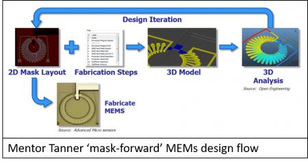
Mentor’s Tanner tools suite takes a different tact. They encourage designers to start with a 2D mask layout of the MEMs and they then combine the 2D layout with a 3D Solids Modeler and a set of 3D fabrication process steps to automatically generate a 3D solid model for FEA simulations. Following this methodology, the 3D structure is iterated using 2D source masks and simulation using auto-generated 3D layouts until the right solution is found. At any point in this process the 2D masks are always in sync with the 3D layout that is being simulated. This avoids the nasty surprise of things not working after fabrication due to masks not creating the right 3D structures. Mentor calls this their “mask-forward design flow” and it differentiates them from the rest of the design flows out there today.
The third step in the process is that once the 3D FEA simulations are working well, the Mentor Tanner flow then makes use of a Compact Model Builder tool that employs reduced-order modeling techniques to create behavioral models from the 3D layout FEA simulation results. These behavioral models can then be used in the final system-level mixed signal simulations to re-verify that the part works as designed before doing the tape-out. This step sounds easy, but without the Compact Model Builder tools it can be extremely time consuming and error prone.
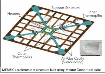 Back to the ingenuity of designers. MEMSIC used this flow to design a 3-axis accelerometer without any moving parts. In the center of the 1mm-square sensor is a heater operating at 100°C above ambient temperature. Around the heater are symmetrically placed thermopiles for reporting temperature in different locations. A thermopile is a series of thermocouples, or temperature-sensing elements, connected in a series to boost voltage. The entire sensor is hermetically sealed in an air/gas cavity, outside of which is analog circuitry for amplification, control, analog-to-digital conversion and, in the 3-axis models, digital compensation/calibration circuitry.
In the absence of motion, the thermal profile is balanced among the thermopiles. But any motion or acceleration modifies the convection pattern around the heater, such that the thermopiles in the direction of the acceleration become hotter than the others. The analog circuitry interprets the resulting signal changes from the thermopiles as motion and acceleration. Wow! It’s like a miniature storm sensor watching the hot gas moving from one side to another as the device is moved. Amazing.
All in all, the MEMSIC guys did a heck of a job with this IoT edge device and the Mentor Tanner guys made it relatively easy for them to do using their fused, analog/mixed signal/MEMs flow. As I said, it never ceases to amaze me as to how ingenious designers can be.
For More details see also:
White Paper: Fused CMOS IC and MEMs Design for IoT Edge Devices
White Paper: MEMs JumpStart Series: Preparing for Finite Element Analysis


Comments
0 Replies to “Fusing CMOS IC and MEMS Design for IoT Edge Devices”
You must register or log in to view/post comments.