Standards have been proven to reduce cost of operations, drive greater process efficiencies and offer greater opportunities for start-up companies to infuse fresh technology in the design and manufacturing of IC’s. Si2 standards have been targeted to resolve “pinch-points” in the overall semiconductor supply chain with a steadfast focus on rapid adoption of these standards.
This day-long program, consisting of 4 individual events, will showcase activities currently underway with an eye towards demonstrating the value of these programs to the program participants and to the overall semiconductor industry. Therefore, this day-long session should entice engineers and technologists working at both current and cutting-edge technology nodes and also managers responsible for driving both design and manufacturing strategy, and related financial and staffing decisions. A featured part of the program will celebrate the 10th Anniversary of OpenAccess.
- A complimentary luncheon and an afternoon reception will highlight this occasion.
- All sessions are free, register here.
- For admission into the Moscone Center you will need to register here for DAC.
- Note that there is a Free Monday option, which will be sufficient to get into the convention hall and then to Room 301. Register here for a Free Pass!
[TABLE] cellspacing=”3″ style=”width: 100%”
|-
| style=”width: 53px” | 09:00am – 10:30am
| OPS Comes to Life
The Open Process Specification (OPS) standard, from Si2’s OpenPDK Coalition, contains all of the data elements that are necessary to create a Process Design Kit (PDK) in any EDA vendor’s or company proprietary design flow. This session is designed to appeal to any engineer working with PDKs and any engineering manager making budgeting or ROI decisions concerning PDK development. It will describe the structure and organization of this very important new standard in the industry and examples of the use cases that this standard will cover.
Presentations:
- Introduction: Jim Culp (IBM)
- Status / Next Steps: Gilles Namur, (STMicro)
- Symbols: James Masters, (Intel)
- Callbacks and Parameters: Gilles Lamant, (Cadence)
|-
| style=”width: 53px” | 10:45am – 12:15pm
| DRC+ – The Next Frontier
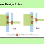
DRC+ augments standard DRC by applying fast 2D pattern matching to physical verification to quickly identify problematic 2D patterns called hotspots In contrast to more time consuming lithographic simulations used after tapeout, DRC+ is transparent to designers as part of their normal DRC checks and it’s fast enough to be inserted throughout the entire design flow.
This award winning technology has been contributed to Si2 and it forms the basis for our next generation OpenDFM standard. This session will cover process characterization, pattern recognition and physical verification using DRC+ acceleration that can be used by any DRC engine.
Presentations:
- Introduction / Quick Refresher on DRC+: Vito Dai (GLOBALFOUNDRIES)
- Standardization Status: SW Paek (Samsung)
- Next Steps: Jake Buurma (Si2)
- Panel: Rachid Salik (Cadence), Vito Dai (GLOBALFOUNDRIES), SW Paek (Samsung), Concetta Riccobeni (LSI), Fred Valente (TI)
|-
| style=”width: 53px” | 12:15pm – 01:45pm
| Lunch: Si2 Open Luncheon, A celebration of the 10th Anniversary of OpenAccess
This complimentary lunch will briefly host the annual open Si2 meeting that will include a short presentation on the “state-of-the-union” at Si2 and announcement of the results of the annual election of Si2’s board of directors. This will be a preamble to the celebration of the 10th anniversary of Open Access. It will cover the road traveled from the genesis of a dream to the reality of today. It will showcase presentations and testimonials, and will recognize key individuals who have contributed to the success of OpenAccess. This event is sponsored by Cadence Design Systems, GLOBALFOUNDRIES, LSI, NanGate, and Spectral Design & Test.
|-
| style=”width: 53px” | 02:00pm – 03:00pm
| New Si2 Standards In Action On Real-World Tools
This session will demonstrate the recently published Si2 Open Process Design Kit (OpenPDK) standards and Open Design for Manufacturability (OpenDFM) standards working with commercially available tools. Si2 standards promote interoperability and these demos are designed to illustrate that point. The demos will show the OpenPDK symbol standard validating the correctness or incorrectness of a schematic symbol change as compared to the standard in real time. The OpenDFM standard will demonstrate an integrated physical verification flow from an electronic Design Rule Manual (eDRM) to XML, to OpenDFM and to four different DRC engines.
|-
| style=”width: 53px” | 03:15pm – 04:30pm
| Standards for a 3D World
Si2 is focusing on developing design flow standards, its area of expertise, to support both 2.5D and 3D designs using through silicon vias (TSV). Specific areas being covered at this time include standards for sharing constraints for power distribution networks, thermal constraints to define such things as “keep-out areas” and constraints to import IP (both dies and blocks) into pathfinding and constraints out of pathfinding into downstream design of individual dies, stacks and interposers. To ensure consistency in standards and to prevent duplication, the Open3D TAB is connected to other relevant groups to ensure a complete solution.
So, this short session will include a presentation of status of activities in the TAB followed by a panel discussion which will include industry experts who will present some of the issues being addressed now and also cover some of the future challenges.
- Presentation: Open3D TAB Status / Next Steps: Riko Radojcic (Qualcomm)
- Panel: Arif Rahman (Altera), Ravi Varadarajan (Atrenta), Aveek Sarkar (Ansys), Keith Felton (Cadence Design Systems), Dusan Petranovic (Mentor Graphics), Riko Radojcic (Qualcomm), Alex Samoylov (Invarian)
|-
| style=”width: 53px” | 04:30pm – 06:00pm
| Si2 Open Networking Reception
This complimentary reception will continue the celebration for the 10th Anniversary of OpenAccess. Free hors d’oeuvres and refreshments will be provided. This event is sponsored by Cadence Design Systems, GLOBALFOUNDRIES, LSI, NanGate, and Spectral Design & Test.
|-