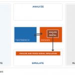
Fergus Slorach, CTO and Founder of Methodics met with me at DAC on Wednesday afternoon to provide an update on software configuration management for hardware designers. Continue reading “Methodics update at DAC”
Methodics update at DAC

Fergus Slorach, CTO and Founder of Methodics met with me at DAC on Wednesday afternoon to provide an update on software configuration management for hardware designers. Continue reading “Methodics update at DAC”
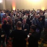
Sunday Night – you have to network at the EDAC kick-off party. Continue reading “Photo and Video Overview of DAC 2012”
Paul Estrada, COO of Berkeley DA met with me on the final day of DAC to provide an update. BDA coined the phrase Analog FastSPICE and have continued to dominate that market segment in the world of SPICE circuit simulators. Continue reading “Analog FastSPICE update at DAC”
Ed wrote recently about Microsoft going thermonuclear. I think that they already did. Ed wrote about Microsoft’s tablet announcement. The second announcement is a sort of follow up to my blog on what will happen to Nokia.
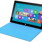
Two big announcements, the first one is that Microsoft is going to produce its own tablet computers (MiPads although they are offically called Surface). A low end ARM-based one and a high end Intel-based one. Daniel Payne was ahead of me at DAC bringing just his iPad and a keyboard (the MiPads have keyboards too) and leaving his laptop at home. I guess he’s not that far away from not bothering to buy a new laptop. So Microsoft is going full-bore to compete with its licensees, at least in laptops/ultrabooks.
The second big announcement…actually not big, they tried to downplay it…is that any WP7 cell-phone will not be upgradeable to WP8. This means that carriers will simply not sell WP7 based cell-phones. Not that they were really doing anyway. Nokia (the only significant Microsoft licensee) is down to 2% market share, and the other licensees (Samsung, Huawai, LG) all have Android phones and, in the case of Samsung, two more of its own operating systems. Is this significant? Well, here’s one datapoint: T-Mobile in Germany immediately announced it is not going to sell the Lumia 900…despite the fact that they have already been advertising it. Remember, in cell-phones, it doesn’t matter if your operating system is any good, just whether the carriers will sell it. And T-Mobile may be an also-ran in the US but they are Germany’s biggest carrier.
The official Nokia response from Elop himself:We have a lot of exciting capabilities coming as part of a pattern of updates for the existing Lumia products. This includes some of the most significant visual elements of WP8 – for example, the new start screen. As we have always been, Nokia is committed to delivering a long term experience to any purchasers of our products.
Count me underwhelmed.
My read: Microsoft has realized they are dead in cell-phones. The Nokia strategy has failed and all the other carriers are fed up of being screwed by non-upgradeable Micosoft operating systems: Windows Mobile to Windows Phone, not upgradeable. Windows Phone to WP7, not upgradeable. WP7 to WP8, not upgradeable. Fool me once, OK. Fool me three times, no way.
If Microsoft is not going to gradually decline into obsolescence (iPhone alone is already bigger than all of Microsoft) then they have to succeed in tablets. I guess they don’t feel that they can compete if they have to rely on their licensees (after all, how did that work for PCs…oh yes, incredibly well, they stole all the profit that Intel didn’t get) so they are going to do it themselves.
Microsoft has a mixed record in hardware. Some very successful products (early mice and keyboards, Xbox) and some total duds (Zune, Kin—the shortest lived cell-phone ever). But none of these (maybe Xbox a little bit) didn’t compete with their PC partners. Now they have launched what could turn out to be an all-out war. It may look minor, just like Anschluss in 1938, when Germany invaded Austria, but it will have huge repercussions. And if Microsoft gets into tablets, what about its own phones too, a smart-phone is just a small tablet with a chip added from Qualcomm, after all. Except for that carrier relationship thing…remember, the carriers hate Skype=Microsoft and with the lack of upgradability they hate them again. But won’t the MiPads also need carrier access. Well, yes, but for now they are WiFi only without also having the blazingly fast LTE access of iPad3 (sorry, the “New iPad”).
So what will happen? Prediction #1 the board will fire Elop as CEO of Nokia and the new guy will abandon Microsoft (after all Microsoft has already abandoned them). As Tomi points out, Nokia has three other operating systems:
Prediction #2: WP8 will have trouble finding tablet licensees. Dell, Lenovo etc already all have Android offerings. Where people have a choice, they don’t see Microsoft as a good one. And why wouldn’t the manufacturers want Microsoft. Oh yes, they took all the profit last time and that’s not going to happen again.
I met with Jay Madiraju of Mentor Graphics on Wednesday at DAC to get an update on their AMS simulation products. We worked together at Mentor back when Mach TA was being developed as a Fast SPICE circuit simulator.
Continue reading “AMS Simulation Update from Mentor Graphics at DAC”
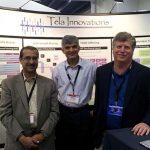
Rajiv Bhateja, Dhrumil Gandhi and Neal Carney met with me at DAC on Wednesday to give an update on what’s new in 2012 for Tela Innovations, a provider of lithography optimized IP and tools. This team has a rich history in EDA and IP from companies like: ARM, Artisan, Mentor Graphics and Silicon Compilers. Continue reading “FinFET Standard Cells at DAC”

At the TSMC Theater Apache (don’t forget, now a subsidary of Ansys) talked about Emerging Challenges for Power, Signal and Reliability Verification on 3D-IC and Silicon Interposer Designs. The more I see about the costs and challenges of 20/22nm and below, the more I think that these 3D and 2.5D approaches are going to be one of the main ways that we keep on the Moore’s law curve at the system level.
There are lots of challenges for 3D designs:
Of course Apache is not directly involved in all of these, just the last 4. Apache have proactively been working with TSMC on these issues both for regular 20nm designs and for 3D designs.
One of the most recent changes is the addition of more complete thermal analysis. This is then fed back into the power analysis (because high temperature affects performance which affects power which affects temperature…, not to mention it accelerates metal migration and other reliability issues). RedHawk is used to generate the Chip Thermal Model (CTM) which is fed into Sentinel-TI also with input from IcePick system thermal tools (to analyze heat flow out of the package etc). This combination makes very accurate thermal analysis, and thus the way that this effects performance ane reliability.
Apache/ANSYS have been working closely with TSMC for 3D designs that combine power analysis from Apache with TSMC’s DFM Data-Kit (DDK) modeling to arrive at a complete analysis of a stack of die on an interposer in a package with heatsinks, in-package slugs etc.
One specific problem in the short term is analyzing Wide I/O since JEDEC has standardized wide I/O for memories meaning that there are lots of signal integrity issues, especially using Wide I/O on silicon interposer (where there is lots of routing involved too). The same problems arise with any wide bus, and wide-buses are common on 3D and interposer designs since the ability to have almost as many “pins” as you want is one of the advantages of 3D/2.5D.

Most of what you see at DAC is canned PowerPoint presentations, however on Tuesday afternoon I spotted a company called Oski Technology that was doing something almost unheard of – they had an engineer debugging a digital design from Nvidia using formal tools live. I later found out the engineer found 4 bugs in just three days without any assistance from Nvidia. Continue reading “Finding RTL Bugs Live Using Formal Techniques”

Dr. Raul Camposano, CEO of Nimbic talked with me on Wednesday at DAC to provide an update on what’s new with their electromagnetic simulation tools.
Continue reading “Electromagnetic Simulation Update from Nimbic”
At DAC on Wednesday Rick Stanton of Dassault Systems gave me an update on what’s new with DesignSync, a design data management tool offered since 1998. Rick and I both worked at Viewlogic in the 90’s along with Dennis Harmon who then founded Synchronicity, later acquired by Dassault Systems.
Continue reading “DesignSync update from Dassault Systems at DAC”