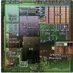
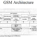
BannerforSemiWiki 800x100 (2)

Apple’s 4G Field of Dreams Build Out

Apple’s 4G Field of Dreams Build Out
by Ed McKernan on 03-30-2012 at 9:00 am

As Apple begins to flood the market with a full line of mobile devices sporting 4G LTE communications capability, starting with the iPAD and soon to follow with Ivy Bridge based MAC Book Pros and then in the Fall with iPhone 5s, one has to ask will the carriers be able to keep pace in order for customers to have a satisfied user experience. I believe there is a critical business model mismatch that will cause Apple to get deeply involved in an accelerated 4G build out and with this a potential new way of servicing its best customers.

Apple has a business model that can be easily summarized by the theme of the movie “Field of Dreams”…. If we build it they will come. In contrast, AT&T and Verizon’s business model is one based on divided loyalties. First: “Don’t shoot until you see the whites of their eyes” because second and more important: make sure do deliver on the quarterly dividend payment.

Imagine Apple, as epitomized by Ray Kinsella, the farmer in the movie who has plowed under his corn field in order to build a baseball diamond that offers the great athletes of a bygone era to relive their past, youthful glories. Fans arrive in their cars from counties wide to enjoy what plans to be a night-time outing. Only the one thing necessary for a game to proceed is missing. The field is not bathing in stadium lights, but by the trickle of lumens emanating from the farmhouse back porch light. You see, the power company is a regulated utility that is more concerned about delivering a nice quarterly dividend on time than it is about building ahead capacity to a new customer. How many night games this summer do you expect to be playing at this field Mr. Kinsella?

The original AT&T, founded in 1885, survived nearly 100 years as a government blessed monopoly churning out a stream of continuous profits in return for guaranteed service to the last farmer residing in the hinterlands of West Texas and the Dakotas. Miles of telephone wires is something an Exec could point to an interested Congressman as a sign of good service to his constituents – no need for more regulation, please. For all the millions of customers who complained about their monthly phone bill, there was an equally vocal crowd of retired investors who counted on the quarterly dividend check to supplement their social security. AT&T was a company where time stood still. It still would be motionless except for the curious, ironic fact that in 1947 its own researchers at Bell Labs discovered the transistor and set in motion the computer industry which seeks to undermine any object (business) that remains at rest.

Don’t misunderstand me; the capital expenditure budgets of AT&T and Verizon are huge. Last year they combined for $65B of new equipment purchases off a $240B revenue base. However, both companies are loaded with debt ($120B in total) that eats up $6.4B in cash (interest expense) and when combined with $16B in dividend payouts, results in a hamstrung business model that is not likely to respond quickly to market demands. With less than a 3% expected revenue growth rate this year, it is hard for any CEO to turn the dial on more capex.

If Apple’s 4G iPAD is intended for part time users of the network, then they may get by with the planned AT&T and Verizon infrastructure improvements. However, if the average user expects to rely on 4G for much of their experience, then the risk becomes one of Apple putting their branding in the hands of a third party who may not care to step up to the plate in a responsible manner. Damaged brand experiences can lead to diminished sales and margins and Apple knows this.

In one of the most interesting passages in Walter Isaacson’s book on Steve Jobs, there was a mention that Jobs wanted to create his own WiFi network to replace the cellular networks so that Apple would have full control over all elements of the phone. In other words, Jobs was concerned about the user experience with cell phone carriers as the gate-keeper.

Given Apple’s current financial position ($100B in the bank growing $10-$15B a quarter) and continued projected double digit revenue gains in the coming year it is incumbent on them to not only guarantee a great user experience (branding experience) but to get a leg up on their competitors. It is easy to draw up a scenario where Apple combines an unlimited 4G data service experience with a closer connection to icloud that drives a monthly commitment. Essentially Apple underwrites carrier capex that is dedicated to these high data customers. The carriers transfer the data charge to Apple who buries it in the icloud bill. As for first users, think of field sales folks who expense it with corporate every month (like they already do with the monthly car allowance).

What does this all mean for semiconductors companies? Perhaps the biggest change will be in how to forecast a communications capex ramp when it goes beyond what the current carriers business models can justify. Upside is definitely possible if Apple makes the commitment to build its 4G Field of Dreams.


FULL DISCLOSURE: I am long AAPL, INTC, ALTR and QCOM


Synopsys Users Group Silicon Valley 2012 Keynote: ARM

Synopsys Users Group Silicon Valley 2012 Keynote: ARM
by Daniel Nenni on 03-28-2012 at 12:49 pm


Keynote #2 at SNUG 2012 was John Cornish, VP Marketing at ARM. Why they sent a marketing person to speak in front of 2,000+ engineers I do not know. To top that, next time they should send a sales person and do a real dog and pony show. To find out more about John I checked his LinkedIn profile which was bare. So enough about John, lets hit on the key points of his presentation:

[LIST=1]

  • The world is mobile and connected
  • Energy efficient infrastructure is key
  • More functionality in the same footprint
  • Increasing importance of power management
  • The architecture of the digital world is ARM

    Besides pointing out the obvious, John did share some interesting data about Angry Birds and CPU usage. Apparently starting up the game is the big CPU draw but actually playing it, not so much CPU is required. That chart probably tracks with the human brain and how much intelligence is consumed during the same process.

    ARM is pushing the big.LITTLEpower management strategy where you have a little core managing resources while the big cores are only used when required. For example, the NVIDIA Tegra 3 has four big cores and one little core. The ARM Mali GPU is also big.LITTLE. Mike Demler did a nice write up of Mali HERE.

    big.LITTLE processing has been designed to deliver the vision of the right processor for the right job. TheCortex-A15 processoris the highest performing, low-power ARM processor ever developed, while theCortex-A7 processor is the most energy efficient ARM application processor ever designed…

    As an undergrad computer science guy this was known to me as master/slave or asymmetric processing versus a more intelligent symmetric approach where the CPUs were granted equal status.

    There was a lot more to John’s presentation but he lost me to a game of Words with Friends with my wife. I was on a 5 game winning streak so it was a hot and heavy competition, which I lost. My wife and I place some serious bets on these games so it required both my Big and Little processing units.

    With the challenges of scaling 20nm and the coming mobile processor attack by Intel Atom using 22nm FinFet technology, I was hoping ARM would at least mention it. Dr. Greg Yeric, ARM Consultant Design Engineer did a talk on “IP Design and the FinFET Transition”, mentioned in my blog 3D Transistor for the Common Man!, which covered foundry access to finFETs so I know ARM is working on it. It would have been interesting to hear what the ARM SoC FinFet marketing strategy is, especially since the next SNUG keynote is Dr Chenming Hu, the father of the FinFet.

    Here are two other FinFet blogs:

    It will be interesting to see what happens at the TSMC 2012 Technical Symposium next month. My prediction is that we will see FinFets at 20nm as a mid-life kicker. IBM presented two FinFet papers at ISSCC this year so the Fab Club (IBM, Samsung, GLOBALFoundries) will not be far behind.

    As far as trending search terms on SemiWiki: FinFets and 3D Transistors will continue to dominate this year, my opinion, so you will see more blogs on the subject, absolutely.


  • Synopsys Users Group Silicon Valley 2012 Keynote: Aart de Geus

    Synopsys Users Group Silicon Valley 2012 Keynote: Aart de Geus
    by Daniel Nenni on 03-27-2012 at 1:26 pm

    SNUG Chairman John Busco opened the session with a few words about Aart de Geus, the silver anniversary of Synopsys, and some SNUG statistics. A whopping 2,500 people registered this year! Probably due to the Magma acquisition which is prominently displayed on “Welcome Magma Users” signs and on the flat screens which are everywhere. This is probably the last we will here of Magma. From what I have been told the assimilation is complete and less than half of Magma employees were retained.

    John Busco is a good speaker and a very friendly and interesting guy. He made the mistake of connecting with me on LinkedIn a while back so I follow his every move. Since 2002, John has been involved in ASIC design implementation methodology and support at NVIDIA so he is not just a pretty face.

    Aart continued with his theme of Techonomics, where tech meets economics, and Systemic Complexity, where your efforts are not a SUM but a PRODUCT. If at any time, you have a failure or a 0 in your work process the entire product will then equal 0. In the semiconductor ecosystem I have found this to be true, absolutely.

    Aart also introduced a sociodynamic term, “Critical Mass through Collaboration” which may not stick. While it accurately describes a rate of innovation adoption that becomes self-sustaining and promotes further growth, Critical Mass is also a protest held on the last Friday of each month promoting cycling related issues in congested cities around the world. Kind of like the Occupy Movement only with wheels. I rode the SFO Critical Mass before my bicycle accident when a cell phone talking driver ran me down and left me to die like an animal on the side of the road but I digress.

    A more mainstream term would be “Collaboration through Crowdsourcing”. Crowdsourcing is a problem-solving process that involves distributing tasks to a network of people, which would be the “crowd”. SemiWiki is a good example of crowdsourcing. Since going live in January 2011, 233,827 people have visited racking up 2,225,788 page views. Currently SemiWiki has 3,853 contributions from 11,469 registered members in the form of blogs, wikis, and forum discussions.

    Aart made six Magma references, yes I counted, and acknowledged key technical points of Magma products that will be integrated into Synopsys tools in the next 12-24 months. Magma P&R, FineSim, and Silicon Characterization were called out as examples. This supports my previous posted vision that by this time next year Magma products will be just a memory.

    FinFets were mentioned and more importantly the man behind the FinFet technology, Dr. Chengmin Hu, will be keynoting on Wednesday morning. The analogy Aart made is that we are now using 193nm waves of light to draw 20nm lines, which is like using crayons. 3D technology such as FinFets will certainly help but will require 3D enabled tools throughout the design flow. Bottom line, A higher level of abstraction on the design side and 3D modeling on the manufacturing (TCAD) side will be required. Paul McLellan did a blog on Synopsys now in 3D which describes the most comprehensive 3D design offering to date. On the manufacturing side, Synopys is the leader in TCAD so I give them an advantage on FinFets at 20nm and beyond.

    IP subsystems were mentioned (which are also EDA360 ish) and the first such IP subsystem from Synopsys was announced but that is a blog in itself so stay tuned for that one.

    At the press roundtable following the keynote, I asked Aart his opinion on new media and the transparency it’s bringing to the semiconductor ecosystem. Aart sited intellectual property and ethical issues which I agree with 100%. Even though SemiWiki is an LLC, my assets are tied to what I write so I hired an attorney to make sure SemiWiki was fullyFTC compliant, so the evolution begins. Hopefully other websites covering the semiconductor ecosystem will follow suit sooner rather than later. It will certainly help with the signal-to-noise ratio which is also a new media concern.

    One thing Aart and everybody else needs to understand is that, if implemented correctly, new media provides an unfiltered feed back loop that you can either embrace and leverage or ignore and get leveraged by your competitors, just my new media opinion of course.


    Synopsys Validates EDA360?

    Synopsys Validates EDA360?
    by Daniel Nenni on 03-26-2012 at 4:26 pm

    Before I get too snarky here, I would like to thank Synopsys for the invitation to SNUG 2012 and including me with the professional editors at a 75 minute roundtable discussion with Synopsys CEO Aart de Geus. While Aart is not my favorite big EDA CEO (Wally Rhines of Mentor bought me lunch and returns my email), he is definitely the most authoritative CEO within the semiconductor ecosystem. Aart has the breadth and depth of the Synopsys product line to back him and his experience in birthing Synopsys and rising to top of the industry is well documented.

    Continue reading “Synopsys Validates EDA360?”


    Synopsys: now in 3D

    Synopsys: now in 3D
    by Paul McLellan on 03-26-2012 at 8:00 am

    And no red and green glasses required.

    I remember the first time I heard about a Through Silicon Via (TSV), punching a hole through the entire wafer to make an electrical connection at the back, like we do all the time in printed circuit boards with through plated holes. I thought someone was trying one on and trying to make me look a fool. But it is real and becoming realer (as my daughter used to say).

    3D integrated circuits, stacking lots of die on top of each other, is a bit like boiling the ocean. Everything has to change at once. There is little point in being able to circuit simulate a TSV without being able to handle it in place and route.

    Today, Synopsys announced that they were at least heating up the ocean. Their solution involves tools from TCAD to test, from floor-planning (how many floors?) to physical layout.

    In my opinion (which is obviously spot-on) nobody is interested in 3D IC yet. By which I mean punching TSVs through active area and building true stacks of die. The one exception is putting stacks of memory on top of processors and lots of progress has been made here in defining the wide I/O standard whereby you can (or at least should be able) to use any memory vendor you want and switch between them.

    The baby-steps version of 3D is 2½D, namely putting die on a silicon interposer. The big advantage is that the die and their designers don’t need to know a lot about TSVs since there are none in their designs. They exist only on the interposer. There are two big problems with punching TSVs all over a die. One is that they have a huge exclusion area known as a Keep Out Zone (KOZ) and a large part of the reason is that the process of making the TSV stresses the silicon (it uses plasma) leading to threshold shifts in nearby transistors. These are fairly predictable so in the best of all worlds these shifts could be used to advantage, but for sure they complicate doing static timing analysis beyond where anyone wants to go yet.

    Synopsys has been coordinating an effort across their whole tool chain to get 3D ready (as, to be fair, has Cadence and Mentor in the stuff they do). From TCAD tools about how to analyze a TSV, up to higher level stuff like place and route. One area of particular intensity is extraction and analysis: the size of a design can suddenly be many die, and the analysis involve die, bumps, little bonds, interposers, C5 bonds, package pins and even the circuit board. That can be a lot of data.

    One area where there is a problem is thermal. The people who do really accurate thermal analysis can’t cope with the billions of devices on a die-stack. The people who analyze die don’t have the accuracy to cope with multiple die, in multiple technologies, separated by thermally conductive air and micro-balls etc. But this is clearly something where good information is needed. At one level, multi-die stack can be good (every die has another die as a heatsink) but eventually all that heat needs to get out. Synopsys admit that this is a problem they don’t yet address and don’t really have a good answer too even with their partners.

    Another major challenge is test. We never used to worry that much about wafer test, weed out the obviously bad die, package up the rest and throw a few away. When you start to package up multiple die in a package, knowing if a die is good becomes really important. If you are wrong, you don’t just throw away a die that was already bad having spent a bit too much on it, you throw away a set of other good die. So wafer sort, the neglected sibling of test, will become really important. You need lots of known-good die.

    Although Synopsys’s announcement is all about 3D it is really about 2½ because that’s where the real market is today. We will get to 3D (especially if EUV doesn’t work out so we have to go vertical rather than horizontal) but not for a bit yet.

    I can’t make it to SNUG but there are several presentations about 3D there. One from Xilinx, a pioneer in the space, who are shipping a high end FPGA on a silicon interposer, about how they did it. Independent estimates from eSilicon (and to be fair they didn’t have access to Xilinx raw data) reckons they are laughing all the way to the bank compared to trying to build a huge die and get it to yield, an eye-opener to me when I saw the analysis last year at a 3D symposium. 3D is expensive, but big die can be even worse.


    Singapore honors Lip-Bu Tan

    Singapore honors Lip-Bu Tan
    by Paul McLellan on 03-25-2012 at 11:08 pm

    Lip-Bu Tan, the CEO of Cadence, has been named by the Singapore Business Awards as Outstanding CEO (overseas) last week. These awards were launched in 1985 by the Business Times and DHL, so this year is the 27th year of the award, created to recognize business leaders in Singapore and abroad.

    As it happens, Cadence flew me first class to Singapore and put me up in the top hotel in town to cover this event…I wish. But as it happens I am indeed in Singapore but under my own steam.

    I don’t know Lip-Bu’s history personally, but he has an undergraduate degree from Nanyang University in Singapore and then an MS in Nuclear Engineering from MIT and an MBA from USF. So I guess like so many people he came to the US to do his master’s degree and, whatever plans he might have had, he ended up staying here (I came to the US in 1982 for “a couple of years” with the plan to then return to Britain. Doesn’t seem to have worked out that way).

    Singapore is an interesting country. Of course as a small city state it is comparatively easy to govern but it has many of the problems of larger countries: it is muticultural, with large Chinese, Malaysian and Indian populations. But nevertheless it has gone from having sub-Saharan African levels of per-capita GDP to be in the top ranks ahead of many European countries. It is generally regarded as having one of the best civil services in the world, and they famously encourage really bright people to join by paying some people 7 figure salaries at the highest ranks.

    I think Li-Bu has done a good job under very difficult circumstances taking over Cadence after the Intel team blew it up, and getting it back to health. So I don’t want to take anything away from him by wondering how many Singapore expatriates are running overseas companies. Again, Singapore is a small country (5M people) and so it is not surprising that when you think of CEOs in the US who came from overseas there are lots of Indians and Chinese (which are both over a billion people so encompass between them nearly 1/3 of the world).

    And surprisingly, Switzerland, at nearly 8M people another small country not noted for the large number over overseas CEOs, nonetheless was the origin of Aart de Geus, the CEO of Synopsys.

    As I like to point out, I genuinely believe that one of the US’s biggest advantages, one no other country can match and one that currently our politicians are doing as much as they can to squander, is the ability to take the best and brightest from all over the world and have them work effectively and together in ways that never happen elsewhere (the last company I worked full-time for was founded by an Israeli with an Iranian CTO, try doing that in any other country).


    NVIDIA Claims TSMC 20nm will not Scale?

    NVIDIA Claims TSMC 20nm will not Scale?
    by Daniel Nenni on 03-25-2012 at 6:00 pm

    Interesting article from Joel Hruska on ExtremeTech: Nvidia deeply unhappy with TSMC, claims 22nm essentially worthless . The title is a bit dramatic (poetic license) but the charts are accurate to the degree that 20nm costs will be significantly higher from the start and will continue to be higher throughout production and maturity.

    One reason is double patterning, which is required at 20nm (double patterning splits a design into separate masks when devices are too close together). If 28nm masks cost $3M, 20nm masks will cost $5M or more. Another reason is design complexity: layout dependent effects (LDE) and process variation will get worse at 20nm, simulation and verification requirements will explode, and the list goes on…

    Life in the semiconductor ecosystem certainly gets more complicated when you try and cram 30B+ planar transistors on one chip, absolutely!

    There is no doubt in my mind that these slides are authentic. NVIDIA CEO Jen-Hsun is quite the showman and has a reputation for this kind of public grandstanding. I was a little surprised that NVIDIA used some sort of “normalized” $$$/transistor as a key metric, rather than more traditional semiconductor scaling measures, but perhaps that’s part of their internal business model.

    One thing you must know, Jen-Hsun Huang and Morris Chang are VERY close, so you have to play a game of chess here and ask yourself what the agenda really is. A public whipping such as that? Openly criticizing your good friend and founding business partner?

    Check out this video at the Silicon Valley Computer Museum, Jen-Hsun interviews Morris, it starts at 8:30 minutes in:

    This video will give you a good understanding of the relationship between Jen-Hsun and Morris. It also provides a candid view of Jen-Hsun’s personality, which seems somewhat narcissistic to me.

    This topic is certainly timely since the annual TSMC 2012 Technical Symposiumwill take place on April 17[SUP]th[/SUP] at the San Jose Convention Center. Trust me, you’re not going to want to miss this one!

    Join the 18th annual TSMC Technology Symposium and get first-hand updates on TSMC’s advanced and specialty technologies, advanced backend capabilities and future development plans!!

    • TSMC’s 20nm and 14nm process development status including FinFet and advanced lithography insights
    • TSMC’s New High-Speed Computing, Mobile Communications, and Connectivity & Storage technology development
    • TSMC’s robust Specialty Technology portfolio that includes Backside Illumination (BSI), Embedded Flash Power IC and MEMS
    • TSMC’s new and exciting GIGAFAB™ new programs and improvements that enhance time-to-volume
    • TSMC’s advanced backend technology for 3D-IC, CoWoS (Chip on Wafer on Substrate), and Bump on Trace (BOT)

    To me this is a simple case of wafer pricing negotiations gone wild. Since TSMC is in such a dominant position at 28nm and 20nm the industry is telling them, in the Year of the Dragon, to be more like a teddy bear and collaborate on pricing in the same way they collaborate on technology.

    But it’s ridiculous for any fabless semiconductor company to say that they will not aggressively transition to the coming process nodes (20nm and 14nm)! I remember back in the day buying an AMD 40MHZ based PC versus an Intel 36MHZ. Seriously, did I really need that extra 4MHZ? Did I pay extra for it? Of course!

    At AMD’s Financial Analyst Day, CEO Rory Read made a point of saying that the company no longer intends to aggressively transition to new process nodes given the diminishing marginal returns from doing so.
    …….

    Okay, let me clarify, any leading edge fabless semiconductor company that wants to STAY in business will aggressively transition to the coming semiconductor nodes, absolutely. Just my opinion of course.


    SOC Prototyping with FPGAs from a Smaller Vendor

    SOC Prototyping with FPGAs from a Smaller Vendor
    by Daniel Payne on 03-23-2012 at 10:43 am

    The two large EDA companies offering SOC prototyping with FPGA-based boards are Synopsys and Cadence, however there’s a smaller vendor called Polaris Design Systems that also have a product in this important design verification category. I spoke on Wednesday with Rahm Shastry, CEO of Polaris to learn more about this company and vision. Rahm and I both worked together at Viewlogic in the 90’s.

    Continue reading “SOC Prototyping with FPGAs from a Smaller Vendor”


    Intel’s First 14nm Chip NOT an x86 Processor

    Intel’s First 14nm Chip NOT an x86 Processor
    by Ed McKernan on 03-22-2012 at 6:00 pm

    Sometime early in 2013, Intel will tape out its first production chip for 14nm and it won’t be an x86 processor. It’s neither necessary nor prudent to lead with a new x86 processor when the one missing element that the mobile market desperately needs is nowhere to be found: an ultra low power 4G LTE chip that fits under the battery life envelope of smartphones and would be warmly received in tablets, ultrabooks and notebooks as well. Intel’s Eye on the Mobile Tsunami Prize is within reach once its Trigate process is ramped. More importantly the 4G LTE chip will serve as the Tip of the Spear dragging in the Atom processor and graphics solution at a lower power and better economics than what the ARM camp has on the drawing boards (the picture is an IBM 14nm wafer provided by GLOBALFOUNDRIES. Intel did not have one for public consumption.)


    Earlier this year, during Intel’s earnings conference call it was noted that CapEx was increasing to $12.5B in 2012 to enable a Fab footprint by Q4 2013 that is twice as large as what was available in 2011. Many are still wondering how it is to be filled and Apple is one of the educated guesses. Along with the CapEx announcement though was the 21% increase in R&D budget to $10.1B. The increase is so large it will consume the additional profits expected this year. More products are coming, however it seems the best bang for the buck is where the trigate process can solve a problem that the fabless vendors can’t seem to fix at 28nm or 20nm (non-trigate).

    The mystery seems to be solved in the unveiling of Apple’s New iPAD that contains a 50% larger battery in order to handle the increased power consumption of the higher resolution Retina display and the inclusion of Qualcomm’s 4G LTE wireless solution. The battery size grew from 25 Watt hours to 42.5 Watt hours causing the thickness and weight of the iPAD to grow in a direction that I am sure would not make Steve Jobs happy. A compromise was made on the iPAD to win the Screen War, however the iphone is different and not some accommodating to more weight and lower battery life. And so a dilemma unfolds as to how long and by what means will the iPhone receive 4G LTE with its much smaller battery. Unlike today’s smartphone rivals who ship 4G today, Apple has to be careful not to tarnish its brand with a device that shows poor battery life.

    Steve Wildstrom, a veteran PC columnist, recently wrote an article recommending that Apple skip LTE on the next version of the iPhone for reasons of battery life and the presumed lack of benefit of increased data performance. The correct platform to watch movies is the iPAD, which has the larger screen and battery to accommodate the power draw. I agree with the practical conclusions that were drawn here, however with Apple’s competitors surrounding them with 4G smartphones, it will be hard due to marketing reasons alone to hold off forever.

    While the buzz drones on in 2012 over 4G LTE, Intel will force march its engineers to tape out one version of 4G LTE after another until it can sample a 14nm version by no later than early summer 2013 to an anxiously awaiting market. Intel will make the argument to the larger mobile market that they have solved the power issues regarding 4G LTE with a process technology that can operate down to “near” threshold (0.7V) voltages and if a vendor is looking for a competitive edge in the smartphone market, Intel has the answer. The x86 now has a Trojan Horse Platform for undercutting ARM in the mobile space. It reminds me of a strategy penned not too long ago.

    FULL DISCLOSURE: I am Long AAPL, INTC, ALTR, QCOM