RVN! 26 Banner revised (800 x 100 px) (600 x 100 px)

2nd International Workshop on Resistive RAM at Stanford

2nd International Workshop on Resistive RAM at Stanford
by Ed McKernan on 09-20-2012 at 8:02 pm

A Veritable who’s who of ReRAM researchers will be present at the 2nd International Workshop on Resistive RAM at Stanford in the beginning of October. Sponsored by IMEC and Stanford’s NMRTI (Non-Volatile Technology Research Initiative), the program features two days of talks, panel sessions and no doubt lots of networking. The advanced program is online and over at ReRAM-Forum.com, moderator Christie Marrian has some observations on the topics and presenters. While there is a true global presence, there are some intriguing sounding talks from local Si valley companies, Adesto, Intermolecular and Rambus. For more information on the workshop visit www.ReRAM-Forum.com.


Automating Complex Circuit Checking Tasks

Automating Complex Circuit Checking Tasks
by SStalnaker on 09-20-2012 at 7:24 pm

By Hend Wagieh, Mentor Graphics

At advanced IC technology nodes, circuit designers are now encountering problems such as reduced voltage supply headroom, increased wiring parasitic resistance (Rp) and capacitance (Cp), more restrictive electromigration (EM) rules, latch-up, and electrostatic discharge (ESD) damage, which are all sources of possible circuit failure. While none of these effects suddenly appeared in the nanoscale era (sub-130nm), they have become progressively more serious, and must now be addressed during circuit verification to ensure robust designs and reliable operation.

ESD protection is one of the most important reliability issues in today’s CMOS integrated circuit (IC) products. ESD failures caused by thermal breakdown due to high current transient, or dielectric breakdown in gate oxide due to high voltage overstress, can result in either immediate failure of IC chips, or gradual degradation of circuit performance. To obtain high ESD resistance, CMOS ICs must be designed with on-chip ESD protection circuits at the input/output (I/O) pins and across the power lines. Turn-on-efficient ESD protection circuits clamp the overstress voltage across the gate oxide to limit the voltage swing.

The conventional approach to checking such circuitry is to use DRC rules to target areas of a layout that have potential reliability issues to check, which requires adding extra layers called “marker layers” to the IC layout database. Adding marker layers is a manual process, making it ripe for mistakes, and requires additional DRC runs, which extends verification time.

A better solution is provided by a circuit verification tool that automatically identifies the reliability-sensitive geometries and applies specialized physical checks to catch real design problems that impact circuit reliability. The Calibre® PERC™ tool uses information from an IC’s netlist to identify circuit topologies of interest, such as possible ESD paths and probable electrical failure sources, as well as the presence or absence of ESD protection circuits. For example, protection circuits are identified by recognizing device types and connectivity patterns based on any of the ESD configurations commonly known and widely used in designs today (Figure 1). Beyond verifying that the required circuits are present and connected properly, Calibre PERC measures the layout to ensure that interconnects are sufficiently sized to meet a maximum current density requirement. This can be accomplished without the need for marker layers or other manual interventions.

Figure 1. Some commonly used ESD protection configurations

The ESD EDA working group has defined and recommended 39 ESD checks that can be implemented using Calibre PERC to assure a reliable design that is robust against ESD events and electrical failure. In these checks, ESD verification is performed on multiple levels, from cell level to package level, including intra-and inter-power domain ESD checks.

As an example, to implement verification of ESD protection between I/O and power rails, the tool performs the following steps:

[LIST=1]

  • Identify the core circuit that requires ESD protection.
  • Check that the correct ESD protection devices are being used, and are appropriately connected to the core circuit.
  • Check that there are no violations in the ESD protection device connection polarity.
  • Check the sizes of ESD devices against existing ESD sizing rules (to meet current density requirements, clamp width requirements, etc.).

    Since the tool is programmable, ESD checks can easily be expanded to cover parasitic extraction on metal interconnects, and design rule checks on selected ESD topologies, protected circuits, or violating circuits. It can also validate electrical compliance by performing resistance and current density analysis to ensure that the wiring of these devices is robust enough to support the largest currents that can be induced (Figure 2).

    Figure 2. Calibre PERC can address P3P extraction in the physical design, perform current density analysis, and execute design rule checks on identified topologies.

    Automatic voltage propagation of input sources through the design, and voltage-dependent DRC checks, provide additional capabilities to simplify complex circuit verification. For example, the tool can be used to perform advanced electrical rule checks (AERC), which identifies signal lines crossing voltage domains in mixed-signal or multi-domain low power digital designs.

    Additional information about advanced ESD checking can be found in the white paper entitled Solving Electrostatic Discharge Design Issues with Calibre PERC.

    Hend Wagieh is a Senior Technical Marketing Engineer for Calibre Design Solutions at Mentor Graphics. She may be contacted at hend_wagieh@mentor.com.


  • Schematic Capture, Analog Fast SPICE, and Analysis Update

    Schematic Capture, Analog Fast SPICE, and Analysis Update
    by Daniel Payne on 09-20-2012 at 1:10 pm

    At the DAC show in June I met with folks at Berkeley DA and heard about their Analog Fast SPICE simulator being used inside of the Tanner EDA tools. With the newest release from Tanner called HiPer Silicon version 15.23 you get a tight integration between: Continue reading “Schematic Capture, Analog Fast SPICE, and Analysis Update”


    GlobalFoundries Announces 14nm Process

    GlobalFoundries Announces 14nm Process
    by Paul McLellan on 09-20-2012 at 8:00 am

    Today GlobalFoundries announced a 14nm process that will be available for volume production in 2014. They are explicitly trying to match Intel’s timeline for the introduction of 14nm. The process is called 14XM for eXtreme Mobility since it is especially focused on mobile. The process will be introduced just one year after 20nm, so an acceleration of about a year over the usual two year process node heartbeat.


    The process is actually a hybrid, a low risk approach to getting (most of) the power and performance advantages of 14nm without a lot of the costs. The transistor is a 14nm FinFET but the middle-of-line and back-end-of-line are unchanged from 20nm, specifically 20nm-LPM process. So in effect it is 20nm process with 14nm transistors (at 20nm spacing). But this process gets a lot of the advantage of 14nm. It has 56% higher frequency at low operating voltages and 20% higher at high operating voltages. Or the voltage can be reduced by 160-200mV resulting in 40-60% increase in battery life.

    Of course there is not really any area reduction from 20nm since all the metal pitches are the same. But it avoids the cost of having even more layers requiring double patterning and avoids needing to contemplate triple patterning. This is something I’ve been talking about recently, since there is a risk that future processes have higher performance and lower power but not lower cost. In the short term for existing high margin products like iPhone 5 this might not matter much, but in the long run it is the 1000 fold reductions in cost that drives electronics. If we hadn’t had that then we might still be able to make an iPhone in principle but it would cost as much as a 1995 mainframe of equivalent computing power.

    GF have “fin-friendly migration” (FFM) design rules which they reckon should make migration planar designs, especially if they are already in the GF 20nm process that forms the basis for 14XM since only the transistors have changed.

    Test silicon is being run in GlobalFoundries Fab 8 in upstate New York. Like other foundries, GF have been working on FinFETs for years even though they have none in a production process. Because the only thing that is new is the 14nm FinFet transistor, early process design kits are already available and customer product tape-outs are expected next year with volume production in 2014.


    For more information on FinFETs (not specifically GlobalFoundries) here is my blog on a talk from Dr Chenmin Hu, the inventor of the FinFET. It explains the motivation for going away from planar transistors to FinFETs (or FDSOI, the only alternative technology that seems viable at present).


    ReRAM Based Memory Buffers in SSDs

    ReRAM Based Memory Buffers in SSDs
    by Ed McKernan on 09-19-2012 at 11:40 am


    In a paper at the VLSI meeting in Hawaii, Professor Ken Takeuchi described using an ReRAM buffer with an SSD. He points to some major performance gains that one can expect from such a configuration in terms of energy, speed and lifetime. Is this an opportunity for ReRAM that could spur development of the technology? Read more in a post over at www.ReRAM-Forum.com….


    High Speed PHY Interfacing with SSIC, UFS or PCI express in Smartphone, Media tablet and Ultrabook at Lower Power

    High Speed PHY Interfacing with SSIC, UFS or PCI express in Smartphone, Media tablet and Ultrabook at Lower Power
    by Eric Esteve on 09-19-2012 at 10:54 am

    We have recently commented the announcement from MIPI Alliance and PCI-SIG, allowing PCI Express to be used in martphone, Media tablet and Ultrabook, while keeping decent power consumption, compatible with these mobile devices. The secret sauce is in the High Speed SerDes function selected to interface with these high data bandwidth protocol controller, like SuperSpeed USB Inter Chip (SSIC) from USB-IF, Universal Flash Storage from JEDEC and PCIe from PCI-SIG. The second PHY defined by MIPI Alliance: M-PHY, first specified in April 2011 at 1.25 Gbits/s, recently updated (June 2012) to run at 2.9 Gbits/s and a third generation coming next year will hit up to 5.8 Gbits/s.

    You also may read the announcement from the MIPI Alliance: “MIPI® Alliance M-PHY® Physical Layer Gains Dominant Position for Mobile Device Applications”, and see the quote from Joel Huloux, MIPI Alliance Chairman at the end of this post…

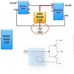
    In order for the information to be complete, the D-PHY (first PHY specification defined by the Alliance) was developed primarily to support camera and display applications, and is now widely used in the systems shipping now. But M-PHY is the function that should be integrated today to cope with the data bandwidth demand in the Gb/s range, and can be compared with SATA 6G or PCIe gen-2, but at lower power consumption. This is the key word for mobile application like smartphones and media tablet, this is exactly the feature which explains why ARM based Application Processor dominates the mobile systems, as strongly as X86 based chipset dominates the PC world-but not the mobile world. In fact, it would be very nice to have actual figures for the M-PHY power consumption, say ay 2.9 Gbit/s on a 28 nm (low power) technology node, and to compare it with PCI Express or USB 3.0 PHY at a similar speed and technology node. I am sure that this information is available “somewhere”, sharing it within the industry could be a good idea…

    According with an analyst quoted in the PR from the MIPI Alliance “MIPI’s D-PHY interface is currently the dominant technology in mobile devices and we anticipate that its M-PHY interface will follow suit.” There is at least a good reason why D-PHY is dominant: if you remember, this function has been created to support Display and Camera interfaces. Display was relying on Low Voltage Differential Swing (LVDS) signaling, a pretty old technology, forcing to use wide parallel busses at the expense of real estate hungry connector, so a serial based solution like D-PHY and the Camera Interface Specification (CIS-2) was welcomed. Camera Controller IC interfaces with the Application Processor was varying with the chip supplier, not a comfortable situation for the wireless phone integrator, so Display Interface Specification (DSI) and D-PHY was also welcomed.

    This explains why CSI-2 and DSI were among the first MIPI specifications to be widely adopted. But the Camera Controller chip makers, integrating the controller on the same IC than the image sensor, on a mature technology node like 90nm, may have some hard time integrating a multi-Gbit/s SerDes on such a technology. The story is slightly different for the Display controller chip, but I suspect the high voltage needed to drive the display to lead to the same situation: mature technology node are not high speed SerDes friendly! It may be that D-PHY will still be in use for some time, to support Display and camera Interfaces, and this is consistent with the feedback from IP vendors like Synopsys, still seeing demand for D-PHY in 28nm…

    Now, we can come to the up-to-date M-PHY, which, as wisely noted by a cleaver analyst “…will follow suit”. To prepare the quote I have made for the MIPI Alliance in the M-PHY related PR, I have interviewed several IP vendors, as I thought their answer would be a good indication about how popular was the function. So, my question was “How many RFQ did you received (for M-PHY)?”, as I knew that asking about the number of design-in, or sales, would not be answered. As they knew that the answer may be published, let’s have a look at the respective answers from Synopsys, Mixel, Cosmic Circuits and Arteris.

    Arteris does not sell any PHY IP, but their Low Latency Interface IP has to be integrated with M-PHY. Arteris is claiming that LLI is used in ten projects, if you consider that the specification has been issued in February this year, that a pretty good adoption rate! Most probably, the fact that LLI allow sharing a single DRAM between AP and Modem, leading to save the cost of one DRAM, is a good enough incentive! Arteris perception of the market is that the AP chip makers prefer using in-house designed M-PHY, at least for the time being. Our perception is that the chip makers adopting LLI are probably the market leaders, and they have PHY dedicated design teams. This may change when the Tier-2 and 3 will also adopt LLI, according with Kurt Shuler, VP Marketing for Arteris.

    This remark from Arteris makes the answer from Navraj Nandra, Director of Marketing for PHY IP products with Synopsys, even more interesting, as Synopsys claim to have had 120 RFQ for M-PHY. Let’s make it clear, a Request For Quotation (RFQ) does not mean that a product will be sold at the end. But that’s a good indication about the market behavior in respect with M-PHY.

    I would like to thank Ganapathy Subramaniam, CEO of Cosmic Circuits, as he was the first to answer (during the week-end), and saying that the company has seen 10+ RFQ for the M-PHY. As far as I am concerned, my estimate would be that the M-PHY could generate up to 20 IP sales in 2012, but I may be optimistic, if we consider that many of the functions will come from internal sourcing…

    The year 2013 could be very interesting to monitor, as numerous functions, like PCI Express, UFS, SSIC on top of the MIPI specific functions like LLI, DigRFV4, DSI-2 or CSI-3, could be integrated and leading to controller IP sales (for the above mentioned IP) and M-PHY IP sales. This could happen, not only for chips used in mobile systems, but also in the traditional PC and PC peripherals segments, as wisely noted by Brad Saunders, Chairman/Secretary of the USB 3.0 Promoters Group: “MIPI’s low-power physical layer technology makes it possible for the PC ecosystem to benefit from the SSIC chip-to-chip interface”.

    Quote from MIPI Alliance Chairman: “M-PHY has truly become the de-facto standard for mobile device applications requiring a low-power, scalable solution,” said Joel Huloux, Chairman of the Board of MIPI Alliance. “We are pleased to join with our partners at JEDEC, USB IF, and PCI-SIG, and MIPI member companies, to advance solutions that push the envelope in interface technology.”

    Eric Esteve – from IPNEST


    Synopsys-Springsoft: Almost Done

    Synopsys-Springsoft: Almost Done
    by Paul McLellan on 09-19-2012 at 8:01 am

    Synopsys announced today that they had completed the two main hurdles to acquiring SpringSoft. Remember, SpringSoft is actually a public Taiwanese company so has to fall in line with Taiwanese rules. The first hurdle is that they have obtained regulatory approval in Taiwan for the acquisition (roughly equivalent to FTC approval in the US, I think). And second, over 51% of the outstanding shares of SpringSoft have been tendered (roughly equivalent to voting in favor of the merger: once 51% shares have been tendered then Synopsys has to purchase the remaining shares and take over the company). Synopsys expects the deal to close definitively on October 1st next week.

    UPDATE: actually Synopsys contacted me to point out that the deal doesn’t actually close on October 1st. They will take control of SpringSoft on that date and will start to consolidate SpringSoft financials into Synopsys financials. The deal will technically close later.

    Springsoft has two product lines that are completely separate except sometimes being purchased by the same company.

    The Laker (Laker[SUP]3[/SUP] is the latest version) product line is a layout editor with a lot of advanced analog placement and routing capability. Synopsys already had a layout capability. Then they bought Magma who had another, reputedly better one. Then they bought Ciranova who had a well-regarded analog placer. Now with SpringSoft they have yet another. I have no idea which technology will survive or how they will merge all this in the end.

    The Verdi (Verdi[SUP]3[/SUP] is the latest version) product line is for functional verification. SpringSoft don’t have their own simulation capabililty but Verdi allows you to manage the verification process and analyze results. Synopsys also have verification environments (not to mention simulators). Again, over time, presumably these technologies will be merged.

    They also have some interesting FPGA-based technology called ProtoLink. This allows FPGA-based verification to be done much more effectively by being able to change which signals are probed on the fly without needing to recompile the entire netlist, which for a big design is very slow. I don’t think Synopsys have anything like it.


    SemiWiki? There’s an App for that

    SemiWiki? There’s an App for that
    by Paul McLellan on 09-18-2012 at 7:20 pm

    The iPhone version of the SemiWiki App is now available. Download it from the iTunes store, it’s free. The App allows you to look at similar things to the website but much more conveniently adapted to fit the small screen. When you first start up the App you can log in (assuming you are a SemiWiki registered user and why would you not be).

    For example, here is the front page of Semiwiki, with all the articles in order. You can, of course, scroll to get to the more articles below. And if you tap on any particular article you get to read it, formatted for the small screen.

    It only went live today so I’m not going to claim that I’ve had extensive experience of playing with it, but it certainly seems easy to use and everything seemed to work as you would expect.

    Daniel Payne did a more detailed explanation of how to navigate within the App here. He was actually discussing the Android version of the App but since they area essentially the same (once you’ve got the App installed) you can read his blog entry and it all applies just the same on iPhone except that to get to the “8 choice” top menu you tap on the “home” button in the middle of the top row. That will get you to here:


    The App is a big advance on just trying to run SemiWiki’s regular website in Safari (or any other browser) where everything is always the wrong size, and it takes more clicks that you would like to navigate around.

    It’s on the App Store here.


    PCI express WILL be used in Smartphone and Media Tablet… opening infinity of new opportunities

    PCI express WILL be used in Smartphone and Media Tablet… opening infinity of new opportunities
    by Eric Esteve on 09-18-2012 at 12:24 pm

    Looking at the various Interface protocols like HDMI, SuperSpeed USB, Universal Flash Storage (UFS) or even SATA integrated in Application Processor for smartphone and media tablet, one extremely powerful Interface protocol, already in use in electronic systems from various market segments from PC, PC Peripherals, Networking, Computing, Embedded to Test Equipment (and I forgot probably some), was still banned from Mobile application, due to the high power consumption of the PCIe PHY layer. As a Semiwiki reader, you are smart and know that I am talking about PCI Express!

    The MIPI Alliance has issued a set of specifications (not a “standard” according with the terminology from MIPI Alliance) that smartphone users are running every time: the most famous are Camera Serial Interface (CSI-2 or 3), Display Serial Interface (DSI, DSI-2), Low Latency Interface (LLI) allowing sharing the same physical DRAM between the AP and the Modem, the list of functional specifications is becoming longer and longer since the creation of the MIPI Alliance in 2003. To support physical data exchange, MIPI defines two types of PHY, D-PHY (half-duplex, up to 80 Mb/s) and M-PHY (dual-simplex, means the protocol can send and receive data at the same time, first defined in April 2011 at 1.25 Gbits/s, an update released in June 2012 runs at 2.9 Gbits/s and a third generation coming next year will hit up to 5.8 Gbits/s).

    M-PHY is the piece which has allowed MIPI Alliance to close deals with:

    • USB-IF, so SuperSpeed USB (USB 3.0) controller can be interfaced with M-PHY, the “merged” protocol is named SSIC, allowing to interface two IC in the system;
    • JEDEC, for the Universal Flash Storage (UFS) support in mobile application, allowing to interface AP with Mass Storage devices.
    • And now the PCI-SIG: the organization will define a new variant of its physical link layer software to run the M-PHY.

    The adaptation of PCIe protocols to operate over the M-PHY is targeted to be released as an ECN to the PCIe 3.0 Base specification and will achieve full integration into the PCIe 4.0 Base specification upon its release. The initial application of this technology is anticipated to be high-performance wireless communications with other applications based on device design requirements. Future implementations are expected in the handheld device market, including smartphones, tablets and other ultra-low power applications. Implementers of this technology must be members of both PCI-SIG and MIPI Alliance in order to leverage member benefits including access to licensing rights and specification evolutions.

    As far as I am concerned, I will probably need to rework this forecast for USB, HDMI, DDRn, PCIe and MIPI!

    For some who remember the blog “Interface Protocols USB 3.0, HDMI, MIPI…Winner and Losers in 2011” the conclusion about PCI Express was: “PCI Express pervasion has been strong in almost every segment (except in Wireless handset, Consumer electronic or Automotive), generating growing IP sales year after year…” Opening the door to PCI Express usage in smartphone and media tablet will create many new opportunities. Like for example to link an applications processor to an external 802.11ac controller. Or, when using the NVM Express specification, benefit from an internal SSD in a media tablet (or smartphone), at a decent cost in term of link power consumption. These are only a couple of examples, but linking these two worlds (everything mobile on one hand, the multiples applications already developed in the PC world on the other hand) will create infinity of new possibilities. Just limited by your imagination power!

    Eric Esteve– from IPNEST

    See here the quotes from the chairman of MIPI and PCI-SIG:

    “We’re excited about the opportunities this collaboration creates for the Mobile industry, MIPI Alliance and its members,” said Joel Huloux, MIPI Alliance Chairman of the Board. “By leveraging our proven M-PHY technology that meets mobile low-power requirements, coupled with the reuse of existing PCIe IP, component and device manufacturers can recoup their investments faster, can drastically reduce the time for product development and validation, and can thus hasten the delivery of innovative solutions to the market.”

    “This collaboration brings together decades of PCIe innovation in PCs with the proven technology of the M-PHY specification that meets the low-power needs of handhelds devices,” said Al Yanes, chairman and president, PCI-SIG. “As PCs evolve to thin and light platforms and tablets and smartphones take on the role of primary computing devices, consumers demand a seamless, power-efficient user experience. We’re pleased to work with MIPI Alliance to deliver a technology solution that meets these demands.”


    ASIC Prototyping with 4M to 96M Gates

    ASIC Prototyping with 4M to 96M Gates
    by Daniel Payne on 09-17-2012 at 9:30 am

    I’ve used Aldec tools like their Verilog simulator (Riviera PRO) when teaching a class to engineers at Lattice Semi, so to get an update about the company I spoke with Dave Rinehart recently by phone. A big product announcement by Aldec today is for their ASIC prototyping system with a capacity range of 4 Million to 96 Million gates, called the HES-7. Continue reading “ASIC Prototyping with 4M to 96M Gates”