The early first generation analog standards all used a technique known as Frequency Division Multiple Access (FDMA). All this means is that each call was assigned its own frequency band in the radio spectrum. Since each band was only allocated to one phone, there was no interference between different calls. When a call finished the band could be re-used for another call, the allocation wasn’t permanent.
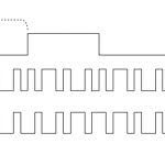
GSM uses a technique called Time Division Multiple Access (TDMA). Despite the mistaken marketing of GSM of providing CD quality sound just because it was digital (it certainly does not), the real advantage of 2G standards was being able to get four times (initially, up to 8 later) as many calls into the same radio bandwidth. Over time it would thus drive down call costs. TDMA works by allocating each call, not just to a particular frequency band as with FDMA, but also to specific time slots within that band. The phones and base-station would only communicate with each other in those slots leaving the other slots free for other calls. With the distances and speeds involved, speed-of-light considerations come into play and the power and precise timing of communication needs to be carefully controlled to ensure that one call does not step on another one in the neighboring slot.
Most of the other technologies that were adopted in competition with GSM were dead-ends, either technically or simply from a business scale point of view. But one technology, used by Verizon and Sprint in the US and all carriers in South Korea, turned out to be very significant: CDMA.
CDMA stands for Code Division Multiple Access. The original version is also known as IS-95 but several subsequent versions were known as CDMA-2000. An explanation of how CDMA works sounds a bit preposterous. Basically all phones transmit in the same band of frequencies at the same time. Since the bandwidth used for the transmission is much larger than the bandwidth being transmitted (compressed voice) it is called a spread-spectrum technology.
So how does a phone pick out the one transmission meant for it from the noise of all the other simultaneous transmissions? That is where the “code” in CDMA comes in. Each phone is allocated a unique code and that code is XORed with the data. The rate of the code is much higher than the data so several bits of code get XORed with each bit of data. The cleverness comes in that the codes are all mutually orthogonal. Without going into an in-depth mathematical analysis of what that means precisely, the effect that if a phone attempts to correlate a call with a different code, it correlates to zero, and if it attempts to correlate with a call using its allocated code then it recovers the original signal.
CDMA is so elegant it is one of those ideas that might be nice mathematically but fail in the real world. After all, signals take different times to reach the phone depending on how far away the base station is, there are reflected signals of nearby buildings and so on. So the transmission has to really be sought out in the received radio signal. In fact received wisdom is that it takes a DSP running at 100 MIPS or more to be able to decode a CDMA signal. The first implementations of CDMA were, indeed, not very reliable.
One of the big challenges is that the power levels of all the radios need to be constantly adjusted so that one with high power doesn’t overwhelm ones with lower power like everyone at a party trying to talk louder than everyone else. The code approach only causes partial rejection of incorrect signals and an excessively powerful one may get through.
CDMA is a technology created from whole cloth by one company, Qualcomm, based in San Diego (actually La Jolla). They created the technology, patented it, licensed it to semiconductor manufacturers and cell-phone manufacturers, and even at the beginning had a joint-venture with Sony to manufacture phone handsets to kick start the market.
In practice, Qualcomm was the company that understood CDMA and had all the rights, so it was hard to build CDMA phones except by buying chips from Qualcomm. Riding this wave, Qualcomm has risen to be a top-10 semiconductor company, still fabless. Today TSMC manufactures most of their chips
The reason that Qualcomm and CDMA have turned out to be so important is that 3G standards are largely based on Qualcomm’s patents. CDMA makes more efficient use of wireless spectrum (which is the bottleneck resource) by the way the power levels dynamically adjust. In comparison, TDMA cannot adapt by packing 5 calls into a channel instead of 4 if radio conditions are good and there are no channels left.
W-CDMA (Wideband CDMA) is a generic term for a number of wireless technologies all based on Qualcomm’s fundamental technology although initially developed by NTT DoCoMo in Japan. It is the basis of all European and US 3G standards. The Chinese TDSCDMA is also based on the same approach, although supposedly designed to get around Qualcomm’s patents and thus avoid the royalties that all other manufacturers pay. Qualcomm claims it still infringes many patents but since the phones only work on one network in China, China Mobile, and have no export market there is little they can do.
The big change in the 3G era was the arrival of smartphones. Responsive data access suddenly became important, not just the capability to make voice calls. Data is very different from voice in a couple of ways. Firstly, voice is a fixed data-rate and there is not really any advantage to transmitting it faster, just more efficiently. Data is not like that, everyone really wants gigabits of bandwidth to their phone if they could get it. Secondly the reliability requirements are higher. If a packet of voice fails to get through it is not worth retransmitting it, better to have a few milliseconds of silence (or comfort noise) in the middle of the call. But data is not like that, and usually every packet needs to be retransmitted until it successfully gets received.
As a result, in 2/3G standards, voice is circuit switched and a dedicated special channel is set up for each call, whereas data is packet switched without a dedicated radio resource for each data circuit.
There were expected to be a number of 4G technologies, in particular Qualcomm’s successor to CDMA2000 called UWB (Ultra-Wide Broadband). But Qualcomm stopped development of the technology and threw their weight behind LTE.
LTE stands for Long Term Evolution (only an international committee could pick a name like that). Actually what current marketing by cellular operators calls 4G is often called 3.9G inside the mobile industry. In fact there are so many standards with different capabilities that it is almost arbitrary where they are broken into generations. So the current generation is now called 4G and the next generation is meant to be called “true 4G” but don’t hold your breath.
LTE is an evolutionary development of the GSM standard by way of W-CDMA. It is incompatible with 2G and 3G systems and thus needs dedicated radio-spectrum. Initially CDMA operators were expected to have their own 4G evolution, but in the end they too have decided to migrate to LTE.
Until LTE, all standards were a sort of hybrid, with digitized voice handled differently from digital data such as internet access. LTE is a flat IP-based approach where voice is compressed into digital data as before, but no longer has a dedicated circuit-switched mode of transmission; it is simply transmitted over the data channel like a “voice-over-IP” phone service such as Skype.
The transition to LTE is complicated by the need to keep phones working in all areas as the LTE build-out proceeds. The most common approach is to use LTE for data when it exists and fall back to the 3G data when it does not. Meanwhile, voice calls are still circuit switched through the existing 3G system (GSM or CDMA). Depending on the architecture of the handsets and the network, it may or may not be possible to both make a voice call and have data access at the same time.
Eventually, when all areas have LTE base stations and all handsets support LTE, it should be possible to shut down the legacy circuit switched infrastructure and use the freed-up spectrum for more LTE bandwidth.
That is where we are today. In large metropolitan areas LTE is up and running. Smaller markets will transition more slowly. State-of-the-art smartphones such as the Samsung Galaxy S3 and the iPhone 5 have LTE data access but still circuit switch the voice. Unless using an over-the-top (OTT) voice service such as Skype that simply re-routes calls through the data channel (and bypasses the carrier billing for a voice call).
One challenge for carriers is that they have got used to charging much more for a voice call (and a text message) than the equivalent amount of data. For example a GSM Enhanced Full Rate vocoder compresses voice into 12kb/s. And into nothing when you are not talking, which is about half the time (because you are listening). A 3GB/month data subscription costs about $20-30 but can handle about 1000 hours of calls (as data) without exceeding the data cap. But 1000 hours is more hours than there are in a month. You literally cannot exceed gigabyte sized data caps with voice calls. But a user with several thousand minutes per month of voice calls is paying about ten times as much until now.
Also see: A brief History of Mobile: Generations 1 and 2