CEVA is happy to welcome new competitor in the DSP IP solution for Computer Vision and Imaging elitist club! In fact, we all know that the competition is not only good for IP customers, but is also a good way to boost innovation and propose continuously improved solutions, and Computer Vision and Imaging is one field of high creativity, in the Mobile and MultiMedia applications. To be frank, CEVA was feeling lonely since the company has first offered the MM3000 DSP IP solution for Imaging, back in 2010. They have launched the third generation, MM3101, offering multiple enhancements like Power Scaling Unit (PSU) or Integrated AXI, allowing to build best-in-class solution in term of power consumption and TTM through easier integration, both being key differentiators in the Mobile industry.
As Paul McLelan has explained in a brilliant post, processing the algorithms for Image Enhancement, like Video Stabilizer, Local DRC, HDR or Super Resolution, and Computer Vision, like Face Recognition, Gesture Recognition, Gaze Detection or Forward Collision Warning, is simply not possible anymore on ARM CPU core or even GPU core: the associated power consumption is far too high, in the multiple Watt range, when the allowed power budget is in the mW range! Clearly, DSPs as a more viable option than offloading imaging and vision tasks to a GPU, which has proven challenges with regard to performance, memory bandwidth, die size and especially power. We know that the new paradigm in the SC industry is power consumption rather than pure performance.
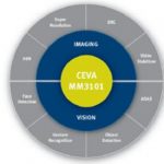
Or I should say, as low power budget as possible to run a specific task, which could demand very high performance level. Let’s take the example of a 32-bit integral image computation on 16b pixel data at 1080p30: the power consumption would be one Watt with ARM core, a few hundreds mW with a GPU core, evaluated to be 10.8 mW by one of our competitor… and less than 3 mW for CEVA MM3101 (at the same conditions: 28nm HPM process, regular Vt). The secret sauce here is: Experience and Architecture. CEVA has built the 3[SUP]rd[/SUP] generation of DSP IP core based on a flexible architecture (see picture). VLIW and SIMD is not enough, the core must be able to be flexible in the operation and not rigid in terms of units doing same operation and capability operating enough units in parallel.
But low power does not mean poor efficiency. Let’s take another benchmark, a normalized cross-correlation function on 16-bit pixel data with 32-bit accuracy. When competition is claiming to achieves 1 million 8×8 blocks per second, CEVA has demonstrated one order of magnitude better performance, with 12 Million blocks per second!
Once again, there is a secret sauce here. CEVA integrates a Power Scaling Unit (PSU), able to provide as much power as needed during computation, and drastically reduce power after. Such a technique could be implemented by SoC designer, but would take time, so, when CEVA provide it in their solution, it’s better for TTM! As well, CEVA standard solution for Imaging integrates AXI Bus, as well as Memory and Control cache management, so the SoC designer just need to select and integrates the memory… Once again, shorter design cycle allows better TTM!
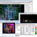
CEVA will show several demos, built by their customers, like Gesture Recognition and Tracking, Face Recognition, or Lane Departure Warning (LDW) for Advanced Driver Assistance Systems (ADAS) applications, to name only a few. This also means that CEVA DSP IP Imaging solution is Silicon proven. But if you need a development board to build your own demonstrator, it’s available from CEVA, as you can see on the picture below.
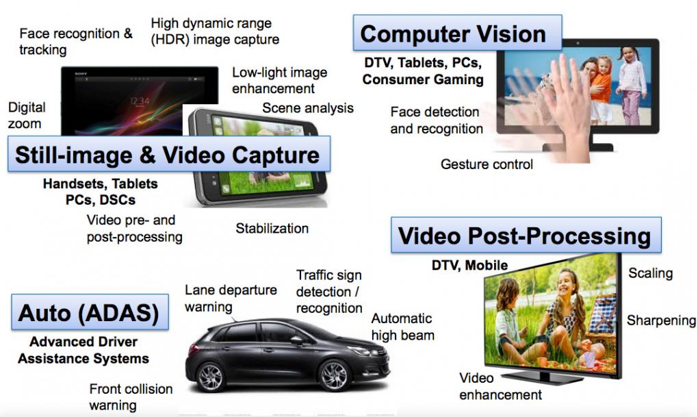
Just to finish, let’s mention that CEVA solutions for Imaging and Computer Vision are implemented in multiple application, starting with Mobile, which is probably the largest market, up to MultiMedia or Surveillance.
Eric Esteve from IPNEST –