Samsung’s aggressive marketing is starting to hit the fabless semiconductor ecosystem so we had all better be prepared. Samsung’s 2012 marketing budget exceeded $400M which probably beats the marketing budget of the entire fabless ecosystem! The question is, will the fabless semiconductor industry be easily swayed by Samsung’s clever marketing? Let’s take a look at their recent mailer and see:
Samsung is fueling the innovations that are changing the way we connect, interact, and benefit from technology. Our low-power, high-performance components and advanced process manufacturing are the foundation for your next leap in mobile products and the infrastructure that connects them. Connect with Samsung and stay abreast of our latest solutions.
This email talked about 14nm and getting ready for FinFET design. According to what I hear in Silicon Valley, Samsung is claiming to be far ahead of the competition and that is confirmed here:
GET READY TO DESIGN 14nm PROCESS IS HERE!
- Samsung partners’ ARM, Cadence, Mentor, and Synopsys, have already successfully taped out multiple test chips
- Learn how Samsung’s new 14nm FinFET process can boost performance and lower power in your next mobile chip design.
- Download the latest 14nm process FinFET technology brochure.
The foundry business is all about setting customer expectations and meeting them. Let’s take a look back at 28nm. According to an EETimes article dated 6/6/2011:
South Korea’s Samsung Electronics Co. Ltd. said Monday (June 6[SUP]th[/SUP]) that its foundry business, Samsung Foundry, has qualified its 28-nm low-power (LP) process with high-k metal gate technology and is ready for production.
Where is the qualified 28nm silicon they speak of almost two years ago? Why does my iPhone5 have a Samsung 32nm based SoC? Why does TSMC have 99.99% 28nm market share? If you want someone to blame for the 28nm shortage how about Samsung? Clearly they did not deliver. Barely a month later (7/12/2011) EETimes reports:
Samsung Electronics Co. Ltd. has said that is foundry chip making business has taped out an ARM processor test-chip intended for manufacture in a 20-nm process with high-K metal-gate technology.
Where is the Samsung 20nm silicon they speak of? I’m waiting for a teardown of the new Galaxy S4 but knowing that the S3 is powered by a 32nm Samsung SoC I highly doubt we will see a Samsung 20nm SoC anytime soon.
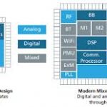
Speaking of marketing smoke and mirrors, I was at the Samsung keynote at CES where the Exynos 5 Octa SoC was launched claiming to be the first (8) core SoC. There was a more technical presentation at ISSCC a month later. In reality, the Exynos 5 Octo is (4) off the shelf ARM A15 cores plus (4) off the shelf ARM A7 cores in a Big/Little configuration where only (4) cores can be used at a time. What a mess, they should have named it Octomom!
Meanwhile, back on planet Earth, Apple and Qualcomm license the ARM architecture and create highly integrated custom SoCs tuned for the associated operating system, which is why they have the best performance/battery life ratio on the market today. How long until APPL and QCOM have the ARM 64 bit architecture rolled out? Closer than you think, believe it.
Time will tell but based on previous Samsung marketing materials for 28nm and 20nm, Samsung 14nm may not be as close as it appears. Samsung 28nm test chips were announced June of 2010 and hopefully we will see 28nm production silicon 3 years later. Samsung 20nm test chips were announced July 2011 with silicon expected in 2014? Samsung 14nm test chips were announced in December of 2012 so you do the math. Maybe Q1 2016? If so they are behind the competition, certainly.
Of course that will not stop the Samsung propaganda machine. As they say, the pen is mightier than the sword and $400M buys a whole lot of ink!