There’s a one-person EDA start-up called iSchematics.com that offers schematic capture and cloud-based simulation for both web browsers and mobile devices like the iPhone and iPad that is being sued. I’ve blogged about their EDA tools before:

Mobile Storage Interfaces: There are a Lot
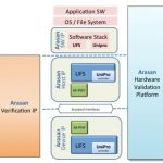
Storage interfaces for mobile are evolving rapidly, in particular with the Universal Flash Storage (UFS) standard. So how do you test a design? If you want to test a design that accesses, say, an SD card then you can wander into Fry’s and buy an SD card for a few dollars. But to design an interface to UFS is a bit harder since the devices don’t yet exist, nor does test equipment like protocol generators.
I was at the JEDEC mobile memory conference last week and listened to Yuping Chung of Arasan talk about UFS and verification.
Universal Flash Storageis a JEDEC standard for high performance mobile storage devices suitable for next generation data storage. The UFS is also adopted by MIPI as a data transfer standard designed for mobile systems. Most UFS applications require large storage capacity for data and boot code. Applications include mobile phones, tablets, DSC, PMP, MP3, and other applications requiring mass storage, boot storage, XiP or external cards. The UFS standard is a simple, but high-performance, serial interface that efficiently moves data between a host processor and mass storage devices. USF transfers follow the SCSI model, but with a subset of SCSI commands.
A UFS controller has two major challenges: interfacing to UFS and maintaining backwards compatibility with the older standards (which also have not stopped evolving). Assuming that you are building something like an application processor (AP) for mobile then you want to know you have all those standards nailed and your AP will be interoperable with whatever it needs to be: e.MMC 4.3, 4.4, 4.5, 4.51, 5.x, UFS 1.0, 1.1, 2.x, UniPro 1.40, 1.41,1.6x, M-PHY 1.0, 2.0, 3.0, SD 2.0, 3.0, 4.0, 4.x, UHS-II…phew, that’s a lot of compatibility.
Of course for most people the sensible thing to do is to license IP blocks for UFS from a company like Arasan. However, that moves the problem from your SoC to Arasan, because they still need to perform verification before seeing silicon (and afterwards, of course). The verification splits into two parts, verifying the M-PHY and verifying the digital controller from layers 2 on up including software drivers.
Separate from the PHY is the rest of the UFS system, which actually consists of two parts, a host controller and a device controller.
Finally, using an FPGA based system the whole system can be validated and software development can be done, ending up with everything that is needed for a successful UFS-based design.
Details of Arasan’s M-PHY are here. Details of Arasan’s UFS solution, including host controller and device controller are here. There is a UFS webinar here(registration). There is a webinar on May 8th at 6pm and 9th at 8.30am (pacific) on Mobile Storage Designs for Compliance and Compatibility – UFS/eMMC, registration is here.
How to Blast Your Chip with High Energy Neutron Beams

So you want to know how reliable your chips are and how susceptible they are to single event effects (SEEs) where a neutron or an alpha particle causes a storage element (flop or memory cell) to flip in a way that alters the behavior of the device. There are two ways a particle hitting a device might not cause a problem. Firstly, the particle might hit an area of the chip that is not vulnerable to particle upsets. Or secondly, an upset occurs but due to other circuitry it doesn’t propagate to an output and thus doesn’t matter.
As with most reliability measures, waiting ten years to find out how reliable a device is over ten years isn’t really very useful. A certain amount can be done in shorter periods and then extrapolating statistically but most of the time this simply takes too long. What is required is a way to accelerate the testing by increasing the rate that the devices are bombarded with particles so that ten years worth of particles can be compressed into a day or two.
There are three types of particles of relevance:
- high energy neutrons (from cosmic rays)
- thermal neutrons
- alpha particles
Alpha particles are stopped by almost anything, just a few centimeters of air for example, so alpha particles in practice have to come from the materials used in manufacture: package plastic, solder, silicon and so on. So alpha particle testing requires the chips to be de-capped or the package would largely absorb them.
Thermal neutrons are generated by a nuclear reactor and so finding it is relatively easy to find a source of low energy neutrons and put your devices in harms way and see what happens.
The most difficult is high energy neutrons. There is no convenient source of high energy neutrons so they need to be made specially at a resource like the Weapons Neutron Research (WNR) facility at Los Alamos. Of course, one immediate question is how do you accelerate a neutron given that at is…well, neutral (A neutron walks into a bar. How much for a beer? For you, no charge.) The answer is that you accelerate protons with a linear accelerator that is a couple of miles long (like the one at the Stanford Linear Accelerator that highway 280 passes over the top of, but much longer). You then put a target in the beam, such as a block of tungsten. This will generate neutrons along with protons and other stuff. So using a powerful electrical field the charged particles can be diverted leaving neutrons. And then using a collimator that is basically a pipe about 12″ in diameter the neutrons that are going in the wrong direction can be absorbed leaving a beam of neutrons.
The beam has a profile of neutron energy that is close to that of cosmic rays, although there are orders of magnitude more neutrons. So if your chip (or system) is put in the beam then it undergoes the effects of years of cosmic rays in a few dozen hours. Since these are single event effects not permanent damage of the device, the chip needs to be powered up and running some sort of test program to pick up the effects when they occur and count them.
As if that doesn’t sound complicated enough, beam time at WNR is booked a year in advance so for an individual company to do this is actually quite risky. If anything goes wrong then you risk missing your beam time slot and having to wait a year for another one.
iROC Technologies does this on a regular monthly schedule so that if you miss your slot with them one month, then you can get a slot the following month. iROC has a lot of experience with this sort of testing, how to set it up, how to execute it, how to analyze the data afterwards. Plus what can go wrong and how to prepare for it so that you don’t waste valuable beam time trying to, for example, find a spare cable.
Which is the best FPGA – Xilinx

Your corporate training will teach you there is no such thing as stereo types and they are bad, naughty. We all know they are true; it’s just some companies now of days try to force the worker bees to do a flash erase and drop your brain at the door. I never participated in that and as you can imagine it went very well. Dilbert is true…
I am asked many many times which is the best FPGA? After pondering for a pico second, I blurt out Xilinx. Flat out Xilinx has the better offering. Now I realize I lost about 47% of you, I’ll call you the 47%’s.:) Now put on your Chuck Schumer glasses and tilt them down so we can have a smart conversation. Try that look in your next performance evaluation and I guarantee you’ll get your 2.78% raise. Who am I kidding; the bucket was much smaller this year, sorry you owe us money.
I have personally seen resistance to the Xilinx product just because ‘We don’t want to be tied to one vendor’. There is some rational for that as I was burned by PA Semi, who wasn’t That was fun. I suggest that Xilinx is so far ahead of the game with FPGA technology that you must choose Xilinx at this point, they are well established and are going no where. And yes, I have programmed Altera. Xilinx has more resources, great IP and is the leader in the field. When the new node comes out, we hear rumblings’ that this is it for Xilinx but they seem to pull it off each time except for that interesting Virtex-4.
What Xilinx needs to be aware of or even nervous about is TOOLS. No one cares if you have the best IP, or 7 Billion transistors if you can’t route them in a reasonable amount of time. I was in a meeting with Xilinx and told them if Altera comes up with a 2x faster router, I’d trade performance for time if the performance is similar. GPUs’ and now CPUs are slowly eating away the market share pie for FPGA legacy systems because they are expensive to design and then route. Then as you know it’s always why is the FPGA not working or not ready, even though they are the heart of the system. I believe Xilinx’s Vivado HLS and Zynq have pushed them into the next level but they need more tools. They need a tool to answer this question for a group of system architects: How do I size my existing system into the Zynq Processor, help me draw that line. Now that is part of my job but companies need a tool to size the system, a quick rough estimate. Without this it is a tough sell to say, look take that Mercury or CW card and put it into this Xilinx part, really?
On the whole, all FPGA companies struggle to say what exactly they are selling. When they talk to us designers it is pretty good, but you know what? I do not have the pocketbook. They need to convey their message much better to program managers and other bosses how they can benefit their program. That is no easy task because as you know, some of these people at this level have had a lobotomy and must follow process at all times and cannot make a decision unless it is in a manual somewhere. Was that a stereotype? :rolleyes:
lang: en_US
Customer Stories at DAC#50

When you think Apache Design you probably think Low Power Design and what stuffed animal will they give away at DAC. The other thing you should think about is how the top semiconductor companies around the world use Apache products for leading edge semiconductor design. Demos are fine, but there is nothing like talking directly to designers who use the tools in an intimate setting (20 people). You definitely do not want to miss this opportunity to collaborate but space is limited so register now:
Experience Sharing by Customers: At-a-Glance
Design experts from AMD, ARM, Freescale, LSI, Nvidia, Samsung, and STMicroelectronics will share best practices and in-depth experiences on how they successfully achieve power, performance,reliability, and cost targets.
Design experts from AMD, ARM, Freescale, LSI, Nvidia, Samsung, and STMicroelectronics will share best practices and in-depth experiences on how they successfully achieve power, performance,reliability, and cost targets.
AMD: Unified Method for Package-Induced Power Supply Droop Analysis in High Performance Processors:
Excessive supply voltage droop can have a significant impact on the clock frequency of high-performance processors. In this work we present a unique approach for power supply droop analysis. A detailed model of the package extracted from layout is combined with a representative model of the IC to simulate dynamic supply voltage gradients across the die. The IC model is geared towards accurate prediction of voltages on power supply C4 bumps. At the same time, it is compact enough to allow efficient simulation of the complete chip-package system. We used this methodology to simulate the droop on a high-performance server SoC. Dynamic simulations were performed with patterns exercising high-power sections of the CPU cores on the SoC. The simulated droops correlate very well with silicon characterizations performed on the same design. We discuss the use of this methodology in future for early analysis of chip/package systems and for driving both IC and package design decisions.
Main products covered: RedHawk
June 5 @ 11:00
To Register
ARM: Comprehensive Power, Noise and Reliability Methodology for ARM Processor Cores:
This presentation will discuss power integrity analysis of Seahawk hard macro, a Quad-core Cortex-A15 implemented in the TSMC 28 hpm process. Seahawk is designed to operate at frequencies close to 2-GHz and has DVFS and retention capabilities built-in. This presentation will describe the power integrity checks that were performed on the design to ensure proper functioning and reliability.
Main products covered: RedHawk
June 4 @ 11:00
To Register
Nvidia: Early RTL Power Analysis and Reduction for Advanced Low-Power GPU Designs:
This presentation covers Nvidia’s methodology for RTL power analysis and reduction using PowerArtist. Data on PowerArtist RTL power correlation vs. sign-off tools will be presented along with runtime performance metrics. Material will also include reports generated using the PowerArtist OADB database API, specific examples of power reduction techniques applied and results achieved, as well as key clock gating coverage and efficiency metrics. In conclusion, this presentation will show key benefits Nvidia achieved with PowerArtist and highlight areas where Nvidia and Apache are collaborating to advance RTL power technology in PowerArtist.
Main products covered: PowerArtist
June 3 @ 11:00
To Register
Samsung-SSI: The Life of PI: SoC Power Integrity from Early Estimation to Design Sign-off:
The life of Power Integrity (PI) analysis starts at the product infancy stage. Early analysis involves resource allocation at the system level, such as the VRM, board, and package, and at the chip level, in terms of power grid structure, power scenario analysis, and the amount and placement of intentional decoupling capacitance (DECAP). This is done through systematic PI modeling and simulation. As the design matures, the power integrity engineer gets more information on the system and on the die. There are many phases of progressive iterations to evaluate design tradeoffs. Power integrity engineers work closely with board, package, and chip design teams to achieve PI closure. At the design tape out stage, the power integrity team is responsible for signing off static and dynamic IR drop and EM to verify that multi-million gates SoC chips meet stringent power supply noise budget. We investigated the impact of board, package, package embedded with DECAP, power grid, circuit switching activity, as well as on-die DECAP and demonstrated good correlation between early estimation and the final analysis with detailed chip and package models.
Main products covered: RedHawk
June 3 @ 14:00
To Register
STMicroelectronics: RTL Power Estimation on ARM Core Sub-systems:
I will start my presentation with an introduction about High Performance Power Efficient ARM Cores implementation within ST and the associated challenge of estimating dynamic power early in the implementation flow. Then I’ll present results obtained when benchmarking PowerArtist tool by measuring accuracy versus signoff power figures on a Dual-cortex A9 subsystem. I will pursue by explaining how we have used PowerArtist tool on a Dual-Cortex A15 subsystem and the different results we have obtained. Finally, I’ll finish my presentation with a conclusion on the benefits of PowerArtist tool.
Main products covered: PowerArtist
June 4 @ 14:00
To Register
GlobalFoundries: Hierarchical Voltage Drop Analysis Techniques for Complex Power-Gated Multi-Domain 20nm Designs:
When qualifying new technologies for new design nodes (e.g. 20nm, 14nm…), large SRAM arrays with many power domainsare employed. Since the VMIN characterization of bit cells performed on silicon requires a sufficient power/ground network, an IR drop analysis at the transistor-level for the whole design is required. This presentation will cover a hierarchical IR drop analysis flow using new capabilities within Totem to trace networks of multi power domains (>800) through switch cells, and to generate subblock abstracts for different detail levels. The abstracts can then be used for top-level analysis; allowing a large speed-up of IR drop analysis in comparison to flat analysis. This presentation also includes a discussion about the pros and cons of the approach and will present resource requirements (run time, memory).
Main products covered: RedHawk,Totem
June 4 @ 12:00
To Register
Nvidia: Comprehensive Layout-based ESD Check Methodology with Fast, Full-chip Static and Macro-levelDynamic Solutions:
This presentation will discuss a comprehensive ESD static/dynamic methodology developed for pre-tapeout ESD verification, failure diagnosis, and predictive simulation of improvements. The methodology focuses on fast, full-chip static and macro-level dynamic analysis and will feature real HBM and CDM application examples. We will also discuss the potential impact of upcoming technologies on ESD including 3D-ICs, FinFETs, and system-level trade-offs.
Main products covered: PathFinder
June 5 @ 10:00
To Register
Freescale: Power, Noise and Reliability Simulation Consideration for Advanced Automotive and NetworkingICs:
This presentation covers experiences of SoCs for Automotive and Networking Applications. Due to the nature of theirapplication domains these ASICs bring different challenges and requirements. This presentation will discuss both Wire-Bond Chips with Low Cost Packaging requirements, as well as high cost Flip-Chip/BGA designs. Instead of discussing typical Power and Rail Analysis details, this presentation will focus on insights gathered from running analysis and silicon results, and will include Power Analysis (RTL and Gate-level), Rail Analysis (Static and Dynamic), handling complicated IPs/Std cells, ESD Sign-off and Cell Electro-migration analysis.
Main products covered: PowerArtist, RedHawk, Totem, PathFinder
June 3 @ 13:00
To Register
LSI: Chip and I/O Modeling for System-level Power Noise Analysis and Optimization:
The system level methodology proposed in this presentation encompasses die, package and PCB interconnects exposing the impact of the capacitive and mutual coupling enabled outside the silicon on the PLL supply. The proposed methodology allows selecting the best package routing solution for PLL supply noise reduction. Correlation with PG noise and jitter lab measurements confirms that our Sentinel-SSO based methodology is critically instrumental in intercepting PLL supply noise due to independently supplied I/O cells switching activity.
Main products covered: CPM, Sentinel, SIwave
June 4 @ 15:00
To Register
Apache Design is a subsidiary of ANSYS, Inc., a leading engineering simulation software provider. Our virtual prototyping technology has enabled customers to predict with confidence that their product designs will thrive in the real world. The extensive ANSYS product suite offers the ability to perform comprehensive multiphysics analyses, critical for high-fidelity simulation of real architecture that integrates varied components.
Apache power analysis and optimization solutions enable design of power-efficient, high-performance, noise-immune ICs and electronic systems. This comprehensive suite of integrated products and methodologies advances low-power innovation and provides a competitive advantage for the world’s top semiconductor companies to help lower power consumption, increase operating performance, reduce system cost, mitigate design risks, and shorten time-to-market for a broad range of end-markets and applications.
Apache technology complements and expands the breadth, depth, functionality, usability and interoperability of ANSYS simulation products. Our combined tools open the door to more comprehensive systems simulation so that engineers can predict product behavior much earlier in the design cycle.
Return to Main Apache @ DAC Page
lang: en_US
A Tale of Two Events, Make that Three, Wait…How about Four?

It is increasingly apparent that Kurzweil’s Singularity is sure getting near, if it is not here already 32 years too soon. Not a week goes by without missing or needing to attend a key conference, seminar, symposium, summit, with each having parallel streams, panels, exhibits, demos, social networking. Not only are we informed, entertained, fed, pampered, enlightened but we get access to post event content, diligent follow-ups, great summaries, blogs, analysis, pictures, all while tweeting and being tweeted with the play-by-play unraveling of the action and pinging of every event. We are to absorb and put in context all this knowledge, we also need to digest, interpret, analyze, identify the relevance to our work and environment, let alone project, extrapolate and derive rules, corollaries and actionable decisions emboldened by this wealth of new information. By the time this settles in our computing neurons, things change and data is so 2 minutes ago.. Now you see the genesis of my Kurzweil lament.
In the last few days, I attended four conferences and I missed four events that I wished I could participate in, if I would have been able to defeat the laws of space-time physics and had the luxury of availability at my disposal. It started with the Linley Mobile Conference followed by the EDPS Monterey event that I and others recently blogged about. This was followed by the Perforce Merge Conference in San Francisco, forcing me to miss Design West and Mentor’s U2U. This week it was AWS Summit and luckily I was able to attend. I have been a cloud fan before cloud was cool, so I was looking forward to it. In some cases the choice of what to attend was easy due to being a sponsor, presenter, or exhibitor. In others it was not as straightforward. Event envy creeps in and anxiety about what new new thing or insight was missed, and hopes rise of getting the recorded sessions and obligatory slide decks in a time delayed fashion.
The AWS Summit had armies of IT and cloud professionals basking in the wealth, breadth and depth of the cloud computing universe orchestrated by increasingly sophisticated implements, tools, pricing and business models rolled out by Amazon Web Services. Andy Jassy, SVP of AWS delivered a Keynote full of content, statistics and guest speakers showcasing accomplishments and results attained through the various AWS offerings.
The Columns above refer to: Replace CapEx with OpEx, lower overall costs, no more guessing capacity, agility/speed/innovation, shift focus to differentiation, go global in minutes.
Andy spelled out how Enterprises are using AWS and the cloud:
- Develop and Test Environments
- Build Apps for the Cloud
- Use Cloud to Make Existing On-premise apps better
- New Cloud App that Integrates Back to On-premise Systems
- Migrate Existing Apps to the cloud
- All-in like Netflix
He went on to outline how to choose a cloud partner
- Experience
- Breadth and depth
- Pace of innovation
- Global footprint
- Pricing philosophy
Great one-liners gleamed from the event:
- There is no compression algorithm for experience
- Sometimes you want to hug your server but it won’t hug you back
The keynote replay can be found here.
lang: en_US
Analog IC Verification – A Different Approach
Analog design seems to suffer from a huge gap when it comes to testing and verification. While some of this gap is natural – after all, often the only way to verify whether a particular design is working is to look at actual simulation waveforms – it still seems like a lot can be done to bring process into this sphere of the IC design space.
Analog designers generally work from their tool GUI’s. Even if they could run automated, or scripted tests to check those parts of the design that don’t need human intervention or bringing up waveforms, it is often hard to get the team to run these tests since they need to be launched from a terminal. In addition, test results are not available from within the GUI.
From a management perspective, analog designs are getting larger, more complex and distributed. One small mistake can cost millions in respins and lost market window. Enabling seamless collaboration across the globe, and tracking team progress is a challenge.
Analog Verification can now be automated using a management console as a new way of looking at testing in the analog/mixed signal design context. A company called Methodics offers a Data Management tool called VersIC with a plugin for Analog Verification management. This plugin for VersIC works in the Cadence Virtuoso 5.x/6.x environments and with the Synopsys Custom Design tools.
Analog IC designers create wrapper scripts to run their ADEXL/ADE/Ocean tests and then use the plugin GUI to register the script and define its required arguments. This is captured in the VersIC database and made available to the entire team
Verification tests can be combined into regression suites, making it easy to run and track a slew of related tests as a single entity. The tool understands all the popular grid management software, so regressions can be launched in parallel, dramatically cutting testing time.
Analog Tests
An analog designer can now automate and keep track of LVS, DRC, power consumption bounds, jitter and leakage measurements. Any kind of ADEXL/Ocean scripted test is a good candidate for this approach. VersIC with the plugin is quite simple to use. Most engineers are up and running in a couple of hours after reading the documentation examples or meeting with a knowledgeable AE.
The alternative to automating analog verification are manual efforts with spread-sheets or writing your own scripts. Using something off the shelf to automate analog tests saves time and lets you concentrate on your core design competence.
VersIC’s SQL database tracks all the tests run across the team – across multiple sites, multiple workspaces, multiple users – making for very effective collaboration.
Now, with a single click, managers can track all the tests run, across their entire team on a given release of a design. You can look at pass/fail rates of individual tests, and even figure out all the design changes that have happened since the last time a particular test passed.
History
The VersIC tool was first released in 2007 and is being used by a mix of large and small companies including: Cisco, Broadcom, PMC Sierra, Motorola, Cirrus Logic, Google, Wolfson, Lantiq, Huawei and ZMD.
Other vendors don’t offer a data management solution with releases attached to a database of the entire test history for that release. In mixed-signal designs this can be combined with the Evolve digital solution from Methodics allowing a single release mechanism for all analog/digital design data with the corresponding verification history.
Summary
Management always has the issue of “what tests have been run and did they all pass” whenever a major release is under consideration. Often “minor” changes to a schematic or layout are included in a release without being properly verified and cause expensive rework. With VersIC’s Analog Verification Management tools, this uncertainty can be removed and design teams can release with confidence, saving hours of manual work per week and helping ensure that silicon is correct.
lang: en_US
Solido CEO on 20nm/16nm TSMC and GLOBALFOUNDRIES Design Challenges

EDA needs more CEOs like Amit Gupta. Solido, which is now profitable, is his second AMS EDA company. The first, Analog Design Automation (ADA), was purchased by Synopsys for a hefty multiplier. Prior to becoming an EDA entrepreneur, Amit was product manager for the wireless group at Nortel and a hardware engineer for the RF communications group at Harris Corporation. I like the Q&A blogs Daniel and Paul do on SemiWiki so here is my first one:
Q: What are the specific custom IC design challenges your customers are facing?
We segment the challenges our customers are facing in the following areas:
[LIST=1]
As you can see, the common theme is that the number of SPICE simulations required to get complete design coverage is exploding, which is leading designers to compromise accuracy to get their designs out sooner, or compromise design time to get accurate results.
Our customers are facing these challenges when doing memory, standard cell, lower power and analog/RF design.
Q: What does Solido Design do?
Solido provides variation analysis and design software for custom IC’s so that our customers can achieve maximum yield and performance in their designs. Solido’s product, Variation Designer, boosts SPICE simulator efficiency while increasing design coverage. Solido Variation Designer is being used by top semiconductor companies to design memory, standard cell, analog/RF and low power custom IC designs at leading design nodes including TSMC and GLOBALFOUNDRIES 40nm, 28nm, 20nm, 16nm.
Q: Why did you start Solido?
This is the second EDA startup I founded – I really enjoy entrepreneurship and the process of starting and building a business to address user challenges. I co-founded Solido in 2005 after my previous company, Analog Design Automation, was acquired by Synopsys. We talked to many companies about upcoming challenges they were facing, and quickly realized that variation in custom IC design was a common theme. We then raised about $10 million in investment capital and worked very closely with lead companies in developing the v1.0 alpha of our product – Solido Variation Designer. Now, we are releasing Solido Variation Designer v3.0 which is in use by top semiconductor companies and qualified by the top foundries.
Q: How does Solido help with your customers’ custom IC design challenges?
Our customers use the following capabilities in our Variation Designer product:
[LIST=1]
Overall, while SPICE simulator companies are focused on improving speed, accuracy and capacity of their tools, Solido is complementarily focused on intelligently figuring out what to simulate giving better design coverage in a reduced number of simulations than brute force.
Q: What are the tool flows your customers are using?
Our customers use Solido Variation Designer with their SPICE simulator of choice. Variation Designer is integrated with Cadence Spectre/SpectreRF/APS, Synopsys HSPICE/HSIM/FineSim/XA, Mentor Eldo, BDA AFS, Agilent GoldenGate. Through our partnership with Cadence, Solido Variation Designer is integrated with Analog Design Environment (ADE), or alternatively our customers input designs through the command line. Variation Designer is integrated with Platform LSF, Oracle Grid Engine and Runtime Design Automation NetworkComputer to run 10’s or 100’s of simulators in parallel. Finally, Solido is qualified in the TSMC, GLOBALFOUNDRIES and STARC reference flows for variation analysis and design.
Q: What is the roadmap for Solido?
We’ve developed a rich custom IC design software platform:
[LIST=1]
Going forward we will continue to work with customers and foundries to address advanced node custom IC design challenges. Having a custom IC design software platform allows us to build new capabilities very quickly and efficiently by leveraging our existing software integrations and enhancing, adapting and inventing algorithmic engines.
Q: Will you be at the Design Automation Conference this year?
Yes, we will be exhibiting at DAC. Readers can sign up here for a Solido Variation Designer demo: http://www.solidodesign.com/
Q: Where can readers get more information?
Some sources of more information:
[LIST=1]
Costello and Hogan Rock the House at Cadence EDAC ECC Event

No one who spent much time at Cadence during Joe Costello‘s reign as CEO (1987-1997, including SDA) could likely give an unbiased review of last night’s event, EDAC – Jim Hogan Emerging Companies Series. The event was held at Cadence’s 5-story Building 10, a building that had not yet been built while Joe was at Cadence. To add some additional character to the event, Joe was interviewed by Jim Hogan, who had worked under Joe at Cadence. But it was Joe and Jim’s discussion on the main topic of telling a compelling company story that kept the audience’s attention.
Most of the readers have likely heard of Joe Costello as he was the leader and face of Cadence during its most explosive growth period. In 1997, Joe was named America’s Top Performing CEO by Chief Executive Magazine. Joe also lead the company into its legal battle with Avant!. Cadence ultimately won that battle though some would say the penalties to Avant! and someof the people involved were insufficient to be a deterrent for future trade secret theft. Joe is tall, about 6’7″, lanky, charming, and has an infectious smile. He is a captivating speaker with a style all his own. I met Joe through the acquisition of Tangent Systems where I was one of the founding team. He is one of the most persuasive people I have ever met.
Looking up at the stage, I could not help but remember how, after I had briefly left Cadence about 6 months after the acquisition of Tangent, I ended up in Joe’s office to discuss my career. After 10 years in developing EDA software and finishing my MBA with the intent to build a career in marketing, Joe, in less than one hour, convinced me I need to work in sales. Looking back, it seems a bit crazy. Sales? I had not sold anything since working at a shoe store in high school. But, sitting in front of Joe it made perfect sense. I’ve heard he knows hypnotism but I do not know if he used it on me. Jim Hogan recounted on stage similar encounters he had with Joe.
Besides the obvious hero worship that many felt, there was some real substance to the event as well. Joe reiterated an approach to building a company story that he had drummed into all of the marketeers at Cadence – write the press release first. By forcing your self to write the press release in advance, you are seeing what you need to support that eventual vision for the company. You are more focused on your goals, the means to get there, and how you will tell the story then. This helps you put together the message now. as this topic came up and it was fun to look around the room and see all the marketing heads nod (Gloria Nichols, Nanette Collins, Michelle Clancy, Jill Jacobs, just to name a few). It was nice to have Joe remind us of the importance of this principle.
I feel I gained a new incite into Joe’s communications ability as well. Joe doesn’t like slides much when giving a presentation. Jim recounted seeing slides with “no white space” and how distracting they could be. Having sat on both sides of the table on investment pitches, neither of them like those meetings that drone on forever in a monotone style. The trick, according to Joe, is you need to “jolt people a bit to get them to stop their linear thinking and see things in a new way.” The discussion on stage then looked at humor as a method to do this. My mind went elsewhere. Joe swears at what sometimes seems to be the most unusual times. It can startle you. It doesn’t seem offensive, especially if you know Joe, but it can be that jolt. And he appears to do it so naturally. So if you are preparing a presentation for DAC… (nah, don’t go there)
In closing, Joe reminded us that although he chose to stay away from EDA after he left Cadence, he is now back. Joe is on the board of both Oasys Design Systems, and another company referred to as Montana (seems like they are still in stealth mode, readers please contribute on this).
This was a truly memorable event for me and I think for most others who attended. Thank you to EDACfor organizing the event, Cadencefor being a gracious host, and to Jim and Joe for being such great speakers. It was well worth the time. And I am most anxious to see what more impact Joe Costello might have on EDA.
lang: en_US
Multi-level abstraction accelerates verification turnaround

Often a question is raised about how SystemC improves verification time when the design has to go through RTL in any case. A simple answer is that with SystemC, designs can be described at a higher level of abstraction and then automatically synthesized to RTL. When the hands-on design and verification activity is at a higher level, there are fewer opportunities to introduce bugs, and it is much easier to identify them before RTL is generated. It’s true that at cycle accurate level of verification, RTL and SystemC will provide the same level of performance, however considering the time required by cycle accurate level of verification, it’s wise to reduce those iterations by doing quicker verification at higher levels of abstractions before RTL. The levels of abstraction in ESL (Electronic System Level) space are very neatly described in a book http://www.cadence.com/products/fv/tlm/Pages/tlm.aspx published by Cadence. Further Cadence has developed a modelled approach to verification methodology which spans through the FVP (Functional Virtual Prototype), HLS (High Level Synthesis) and RTL (Register Transfer Level) levels of abstraction. In the middle of April, in ISCUG conference, Mr. Prashanth G Baddam made a presentation on this methodology, jointly authored by Mr. Prashanth G Baddam and Mr. Yosinori Watanabe.
Prashanth G Baddam, Yoshinori Watanabe
Prashanth very concisely described about what can be verified in the models at each of these levels in order to optimize total verification time, as every item cannot be verified on every abstract model. Hence after the verification plan creation for hardware under verification, categorization of its verification items with respect to the abstract models is important as shown below.
At FPV level, the models are in SystemC programmer’s view with bus interfaces described in TLM2.0. Testbench is single at all levels described in SystemVerilog or e utilizing UVM standard. At HLS level, the model needs to be synthesizable; concurrent blocks for function and refined TLM for communication interfaces. The testbench is extended to verify the interfaces, and to add more tests for the refined functionality. At RTL, the design is closer to hardware with micro architecture details like complete interface information and state transition models. Interfaces are at signal-accurate protocol. The testbench is further extended to use protocol specific interface agents and existing VIPs (Verification IP). More checking specific to RTL is added.
It is evident that at times it becomes necessary to probe values of particular variables, either declared as private members within SystemC module or local to functions for white-box monitoring. As this is tedious to do manually, Cadence provides a library called wb_lib to make this task easy. This library consists of APIs for monitoring local and private variables which can be accessed from the testbench.
Cadence provides a complete metric-driven methodology for verifying any system from TLM to RTL level with powerful coverage capabilities. It provides verification plan editor where verification items at different levels can be identified which get refined as the level moves towards RTL.
With verification starting at the design decision stage, more of it being covered early in the design cycle which is complemented with finer level of verification at later stages and reuse of testbench at all these levels shortens the verification time considerably; 30-50% shorter debug cycle, 2X faster verification turnaround and around 10X faster IP reuse.
The methodology provides broad architectural exploration to gain higher throughput and lower power consumption and size. This also improves efficiency in exploring best verification strategies. The detailed presentation is posted at http://www.iscug.in/sites/default/files/ISCUG-2013/ppt/day1/3_5_MultilevelVerification_ISCUG_2013.pdf
Cadence is closely collaborating with its key customers to tailor this methodology for their specific production environment. That’s encouraging news!!