You are currently viewing SemiWiki as a guest which gives you limited access to the site. To view blog comments and experience other SemiWiki features you must be a registered member. Registration is fast, simple, and absolutely free so please, join our community today!
At the 2025 RISC-V Summit, amid debates over cloud scaling and AI cost, DeepComputing CEO Yuning Liang offered a radical view: the future of intelligence isn’t in the cloud at all — it’s already in your pocket. His lunchtime conversation began with iPhones and ended with the death of the operating system. In between, he sketched a vision of computing that dissolves centralized infrastructure into personal devices, reshaping everything from hardware to human interaction.
Why Do You Need the Cloud?
Yuning waves his phone and laughs. “People keep saying, ‘We need the cloud for AI.’ Why? You’ve already got the compute right here. The only thing missing is space to store your models.” The cloud is no longer the default; it’s just a backup. In Yuning’s framing, bigger storage tiers aren’t luxury upgrades — they’re AI capacity ratings.
He taps on his iPhone’s storage line: “See? 64 gigabytes isn’t just storage — it’s intelligence. You want Whisper for voice, a 7B LLM for reasoning, a vision model for your camera? Fine. They all live here.” Thanks to aggressive model quantization — including FP4 and FP8 formats — today’s smartphones can host multiple intelligent agents. Storage becomes the limit on your on-device intelligence.
William Gibson imagined this in 1988. In Mona Lisa Overdrive, Kumiko carried a pocket-sized Maas-Neotek biochip that projected an AI companion named Colin — visible only to her, contextually aware, able to access local systems and provide guidance. Thirty-seven years later, Yuning is describing essentially the same device. Gibson conjured it decades before we had the silicon to build it.
Today, Yuning argues, correctness is perceptual, not mathematical. If your LLM gets one token wrong out of a million, no one notices. He shakes his head. “In the 20th century, if Intel was off by 0.001 in floating point, it was a crisis. Divide-by-zero? Immediate trap, big exception. That was engineering pride.”
“In RISC-V, you don’t even need to take the divide-by-zero exception,” he says. “Just flag it. Keep running. Why waste cycles pretending to be perfect when the output is statistical anyway?” This mindset shift explains the rise of ultra-low-precision formats like FP4. What matters isn’t IEEE-754 perfection — it’s the human experience.
“The user interface is a relic,” Yuning says. “You won’t open apps in ten years. You’ll forget what a mouse was. You’ll just tell your glasses what you want.” He describes a lightweight AI OS — not an operating system in the old sense, but a runtime that manages models, sensors, and context. One orchestrator that knows who you are, what you’re doing, and loads the right model at the right moment. No menus. No icons. Just interaction.
When the topic turns to silicon, Yuning grows animated. “Everyone’s building SoCs like they’re building cities — giant, expensive, unmanageable,” he says. “I just want to build the brain.” To Yuning, the ideal AI processor is scalar, vector, and matrix compute wrapped around fast SRAM — maybe GDDR6. Everything else (I/O, radios, sensors) is the body. Let the OEMs build the hands and eyes. His job is to supply the cortex.
“The chiplet model fits perfectly,” he says. “Each part is an organ. You snap them together.” This modular vision aligns with the Open Chiplet Architecture, which promotes interoperable compute, memory, and I/O units. Yuning never names OCA directly, but the alignment is unmistakable. “Just make sure the interfaces fit.”
“Everyone’s obsessed with 1024-bit vectors and out-of-order cores,” Yuning says, voice rising an octave. “They’re expensive, they’re hot, and they don’t scale. Why do that?”
Instead, he champions deterministic simplicity. “If you can get the same user-perceived performance with half the power and half the cost, you win. Don’t chase benchmark vanity. Build something that feels fast.”
Here, he echoes a rising sentiment within the RISC-V community — seen in startups like Simplex Micro — that favors deterministic scheduling over speculative execution. Elegance, Yuning suggests, is the new performance metric.
How can a startup survive against Nvidia and Apple? “Do everything with ten times less — people, money, time,” he says. “That’s the rule.” Big companies, he argues, have thousands of engineers managing thousands more. Startups survive by constraint and speed. “We can do in a week what they do in a quarter — if we stay hungry.”
And forget the cloud. “Cloud is not for startups,” Yuning says. “It’s complex and slow. Don’t envy Cerebras or Groq — unless you want to raise money and become another big corporate like OpenAI or Anthropic.” He laughs. “Once you have hundreds of people, thousands of people? You lose the speed. You get all the bad odds — wasting money, wasting time, wasting opportunities. Like government.”
The key isn’t to outspend giants. It’s to out-focus them.
Yuning’s closing prediction: “You’ll wear your computer,” he says. “Glasses, earbuds, maybe a pendant. They’ll talk to each other through local models. No screen, no keyboard. The model is the interface.” The core, he insists, will be a small deterministic brain — not a GPU farm.
The Evaporating Cloud
“Fast, private, local. That’s the future. The cloud becomes the teacher; your device becomes the student. Once it learns, the cloud becomes an artifact.” When that happens, Yuning says, computing will finally be personal again.
Siemens has strengthened its position in EDA and manufacturing by acquiring ASTER Technologies, a specialist in test and reliability solutions for printed circuit boards. The acquisition represents a strategic step in Siemens’ broader vision to deliver a fully integrated, end-to-end digital thread for electronics design, verification, manufacturing, and lifecycle management.
ASTER Technologies is widely recognized for its expertise in design-for-test (DFT), design-for-manufacturing (DFM), and design-for-reliability (DFR) solutions. Its flagship tools enable engineers to validate PCB designs early in the development cycle, reducing costly errors, improving yield, and accelerating time to market. By bringing ASTER’s capabilities into the Siemens portfolio, the company aims to offer customers a more comprehensive and tightly connected approach to PCB test engineering.
The electronics industry is facing increasing complexity driven by higher component densities, advanced packaging, faster signal speeds, and stringent reliability requirements. Traditional siloed workflows—where design, test, and manufacturing considerations are addressed separately, are no longer sufficient. Siemens’ acquisition of ASTER directly addresses this challenge by embedding test intelligence earlier in the design phase, helping engineers identify potential faults before a board is ever manufactured.
From a technology perspective, ASTER’s solutions complement Siemens’ existing EDA offerings, particularly in PCB design, simulation, and manufacturing preparation. ASTER’s test coverage analysis, boundary-scan expertise, and fault modeling capabilities add a critical layer of validation that enhances Siemens’ digital twin strategy for electronics. When combined with Siemens’ simulation, automation, and data analytics strengths, customers gain deeper insight into how their PCB designs will behave in real-world manufacturing and operational environments.
For customers, the benefits are tangible. Integrating ASTER’s test engineering tools into Siemens’ ecosystem enables earlier detection of design issues, improved test coverage, and optimized test strategies. This leads to lower development costs, fewer design re-spins, and higher product quality. Manufacturers also benefit from smoother transitions from design to production, as test requirements are aligned with manufacturing realities from the outset.
The acquisition also reinforces Siemens’ commitment to supporting industries where reliability and quality are mission-critical, such as automotive, aerospace, industrial automation, medical devices, and telecommunications. In these sectors, PCB failures can have serious safety, financial, and reputational consequences. By strengthening PCB test engineering within its portfolio, Siemens helps customers meet stringent regulatory standards while maintaining innovation speed.
From a strategic standpoint, the move reflects a broader trend in the EDA market toward consolidation and platform-based solutions. Customers increasingly prefer integrated toolchains over fragmented point solutions, seeking consistency, data continuity, and scalability across the product lifecycle. Siemens’ acquisition of ASTER positions the company to meet these expectations, offering a unified environment where design, verification, test, and manufacturing data flow seamlessly.
For ASTER Technologies, becoming part of Siemens provides access to a global customer base, expanded R&D resources, and the ability to scale its innovations more rapidly. The combination allows ASTER’s specialized knowledge to be applied across a wider range of industries and use cases, amplifying its impact within the electronics ecosystem.
Bottom Line: Siemens’ acquisition of ASTER Technologies is more than a portfolio expansion, it’s a strategic investment in the future of PCB test engineering. By combining ASTER’s deep test expertise with Siemens’ comprehensive digital industry capabilities, the company is well positioned to deliver industry-leading solutions that improve quality, reduce risk, and accelerate innovation across the electronics value chain.
NetApp recently hosted a webinar on Agentic AI as the future for EDA and implications for infrastructure. Good list of panelists including Mahesh Turaga (VP Cadence Cloud) with an intro preso on infrastructure and agentic AI at Cadence, then our own Dan Nenni (Mr. SemiWiki) moderating, Khaled Heloue (Fellow AMD, CAD CAD/Methodology/AI), Rob Knoth (Sr Group Director Strategy and New Ventures, Cadence) and Janhavi Giri (NetApp Industry Lead, formerly at Intel). Excellent panel with of course views to the agentic future but also grounded guidance on getting into and progressing in adopting AI and agentic. Since this is a long webinar, I won’t dwell on vision, rather my takeaways on near-term observations.
Infrastructure implications
You’d have to be living under the proverbial rock not to be aware that hyperscalers and hopeful hyperscalers are investing huge amounts – hundreds of billions of dollars – in building mega-datacenters. What you might not know (but shouldn’t be surprising) is that 60% of that investment is going into technology development – our industry. What an opportunity for the systems and semiconductor ecosystem!
Mahesh highlighted some of the infrastructure challenge in these datacenters. Racks that once ran at 10-15kW are now climbing to 100-120kW and by 2027 we may see 1-2MW per rack. Already direct-to-chip liquid cooling is unavoidable and at higher power levels we will have to switch to immersion cooling. Further AI-centric dataflow within and between racks now demands microseconds of latency where previously we were OK with milliseconds.
Fast changes in infrastructure with big implications, especially support for design and operations (e.g. scheduling old hardware replacement with new hardware). GPU design cycles run 12-18 months, and hardware must be amortized over 5-6 years, so refresh updates must be carefully planned. Cadence with their Reality Digital Twin works very closely with NVIDIA in helping enterprises design and maintain their datacenters against these and other (thermal, cooling, etc) objectives.
NetApp also play an important role in infrastructure through their management of storage and cloud operations A large enterprise will have design data scattered around the world: US, Europe, India, Asia. And they also want to take full advantage of flexibility in compute/AI options: on-prem, cloud and hybrid configurations. Especially in agentic systems, learning from patterns in distributed data could suggest a lot of complexity and unacceptable performance overhead.
Managing complexity and performance effectively will depend in part on agentic architecture, also on sufficient agentic-aware support from storage and cloud infrastructure. NetApp provides this through an end-to-end data pipeline to find needed data across hybrid multi-clouds, ensure it is current by updating as sources change, provide data governance and security throughout the data lifecycle, and provide support for data transformation as needed by AI apps. All MCP capable (standard for agent communication) and integrated with container orchestration platforms such as Kubernetes.
Panel discussion takeaways
Dan kicked off with a great question: what are the most time-consuming and repetitive tasks that agentic AI could help automate? I like this because it goes to the heart of silly mass media fear mongering while shining a light on the real benefit to engineers (no, engineers won’t be replaced by AI, yes, they will get more time to focus on high-value tasks).
The daily routine of today’s engineer is consumed by low productivity friction tasks: learning how to run unfamiliar flows (especially for junior engineers), scripting through extension languages like Tcl, Skill, Python, figuring out what to do next when something crashes or they aren’t meeting a PPA goal, assembling reports on current progress for the next design review. Necessary but pedestrian work consuming significant time that could be better spent in creatively moving a design goal forward. Task-centric agents together with RAG-based lookup can minimize friction and help junior engineers spin up more quickly. Agentic methods can take this further by automating pedestrian tasks.
We’re still in the early stages of that journey, though in some applications further advanced than others. Driving EDA tools through natural language could be a big advance (I am sure that the next generation of engineers looking back at how we direct tools today will be stunned by the primitive scripting methods we now use). Agentic methods for repetitive analyses would be another obvious win: run analyses for a set of cases together with sweeps across certain parameters and boil down the results, returning the top 3 options worth investigating more closely. Methods that are easy to trust because you are effectively using agentic as a skilled intern capable of learning under your guidance. You can still monitor, check their work, but you don’t have to do the grunt work yourself.
Some of this is already happening, in verification, in floorplanning, in implementation optimization and multiphysics analysis. Still essentially productivity optimization around specific analyses but you could imagine going further. Khaled suggested aiming for fully automating design implementation on simple tiles.
What about risk management? There was consensus that new objectives must be phased in carefully with human supervision. I believe investment here will need major focus on methods to build trust – confidence scoring and “show your work” reports for example – also metrics to monitor how effectively apps are improving productivity and/or QoR. We don’t want to replace pedestrian work in regular flows with pedestrian work in wrestling agentic systems.
Another good question probed how best to train agentic systems. For me this question touches on multiple topics: the architecture of an agentic system in semiconductor/systems design, who should own which pieces, considering need to protect company secrets but also who has the most expertise to train certain agents. Does the nature of these systems promote a trend to an ecosystem of agents and agentic suppliers? For now discussion suggests fairly localized agents augmenting existing solutions, complemented by RAGs as support/lookup mechanisms to answer “how do I…” questions. Not a bad starting point, though maybe we can do a little better by embedding some of that RAG data inside agents.
Lots of food for thought. You can watch the webinar HERE.
The 40-Year Evolution of Hardware-Assisted Verification — From In-Circuit Emulation to AI-Era Full-Stack Validation
For more than a decade, Hardware-Assisted Verification platforms have been the centerpiece of the verification toolbox. Today, no serious semiconductor program reaches tapeout without emulation or FPGA-prototyping playing a central role. HAV has become so deeply embedded in the development flow that it is easy to assume it has always been this way.
But it wasn’t.
With a bit of slack around the exact starting point, this year marks roughly the 40th anniversary of hardware-assisted verification, broadly inclusive of both hardware emulation and FPGA prototyping. Over four decades, HAV has evolved from a niche approach into the indispensable backbone of modern silicon development. Its history is also, in many ways, a mirror of the semiconductor industry itself: as chips grew more complex, as software took over, and as AI began reshaping everything, HAV repeatedly reinvented its purpose.
Long before HAV became a recognized category, there were precursors. IBM, for example, experimented with hardware acceleration through systems such as the Yorktown Simulation Engine and later the Engineering Verification Engine. These machines were essentially simulation accelerators—special-purpose computers designed to run hardware models faster than traditional software simulators. They represented an important step forward, but they remained fundamentally tied to the simulation paradigm. They improved speed, yet not nearly enough to apply real-world scenarios to a design-under-test.
HAV platforms belong to a different class of engines. Early emulators relied on reprogrammable hardware, typically arrays of FPGAs, configured to mimic the behavior of a design-under-test (DUT). For the first time, engineers could interact with a representation of the chip before tapeout at execution speeds approaching real life. Companies such as PiE Design Systems, Quickturn, IKOS, and Zycad pioneered this new verification approach, laying the foundation for what would become a defining pillar of semiconductor development.
The evolution of HAV can be understood across three broad eras: the early years, when hardware complexity first forced emulation into existence; the middle period, when software became dominant and HAV moved into virtual environments; and the maturity era, where AI workloads have driven hardware prominently to the center of architectural innovation.
The Early Years: Hardware Complexity Forces the Rise of Emulation
In the early 1980s, semiconductor designs were defined almost entirely by hardware. Embedded software, if present at all, played a minor role. The industry was driven by pioneers in processors and graphics chips, pushing toward what seemed then an astonishing milestone: one million gates. Verification relied overwhelmingly on gate-level simulation, which served as the universal standard of the time.
As designs grew larger, however, simulators encountered an unavoidable performance wall. Limited host memory forced designs to be swapped to disk, simulation runtimes ballooned, test vector volumes exploded, and the sheer computational load to achieve acceptable fault coverage became unmanageable. Full-system validation before tape-out was becoming increasingly impractical, if not outright impossible. The industry needed something faster, something closer to silicon.
Hardware-assisted verification emerged as a response to this crisis. Early HAV platforms were deployed primarily in In-Circuit Emulation mode. In ICE configurations, the emulator was physically cabled into a live target system, allowing engineers to exercise the DUT in a realistic environment with real peripherals. This was revolutionary. Instead of relying on synthetic vectors, designers could validate chips with real workloads, providing a level of realism that synthetic simulation vectors simply could not achieve. For the first time, verification began to resemble how the chip would behave in the field.
The promise was enormous, but the reality was often painful. Early emulators were complex to setup, finnicky to operate, and prone to frequent failures. Long setup times regularly pushed verification readiness past management deadlines, and reliability issues rooted in cabling and hardware dependencies led to frequent downtime. Mean-time-between-failure (MTBF) could be measured in hours rather than weeks or months, forcing verification teams to spend more effort debugging the emulator itself than debugging the DUT. Even so, despite these frustrations, the trajectory was clear: verification could no longer remain purely software-based.
The Middle Ages: Software Eats the World and HAV Becomes the Verification Backbone
The design landscape changed profoundly in the decades that followed, as functionality began migrating steadily from hardware into software code. This shift was famously captured in Marc Andreessen’s 2011 observation that “software is eating the world.” His prediction proved remarkably accurate across nearly every industry touched by computing. SoCs became software-defined platforms, where intelligence increasingly lived in firmware, operating systems, drivers, and application stacks. Hardware was no longer the entire product—it was the substrate for software code.
This transition transformed verification. Static test patterns were no longer capable of exercising the full complexity of modern designs. Instead, engineers turned to software-driven stimulus, using high-level testbenches to validate behavior across broad functional domains. Hardware verification languages and more abstract methodologies emerged to support this new reality.
HAV engines, once used mainly for real-time ICE validation, adapted by becoming the execution engines behind these software-centric environments. The industry formalized the interaction between software testbenches and hardware-mapped DUTs through transaction-based verification, standardized under IEEE SCE-MI. Rather than toggling signals cycle-by-cycle, engineers could interact with the DUT through high-level transactions, dramatically improving performance and productivity.
This shift also removed many of the practical limitations of earlier generations. Virtualized environments reduced reliance on physical connections and eliminated the need for speed adapters required in ICE-based setups. Verification IP replaced hardware interfaces, enabling scalable, fully digital verification ecosystems.
As the industry embraced “shift-left,” HAV platforms emerged as its most powerful enabler. They allowed engineers to bring up software much earlier in the design process, starting with bare-metal initialization and extending through drivers, and operating systems. Verification was no longer limited to functional correctness in isolation; it now encompassed the behavior of the complete hardware/software system, long before silicon existed.
By this stage, HAV had become much more than a way to make verification faster. It was increasingly the bridge between hardware and software development, allowing teams to work in parallel rather than in sequence, and establishing hardware-assisted verification as the backbone of modern system validation.
The AI Age: AI Restores Hardware Centrality and HAV Goes Full-Stack
From the mid-2010s onward, the industry entered a new era, driven by the explosive rise of artificial intelligence. The narrative evolved beyond software eating the world into something more radical: software consuming the hardware. In the AI age, software does not simply run on hardware, rather, it increasingly dictates what hardware must become. The demands of modern AI models are so extreme that they are reshaping processor architectures from the ground up.
Generative AI exposed the limits of traditional, general-purpose architectures. The enormous data movement requirements and computational intensity of modern models overwhelmed CPUs and strained even highly optimized systems. To keep pace, the industry embraced specialized architectures, including GPUs, FPGAs, and purpose-built AI accelerators designed around massive parallelism and tensor computation.
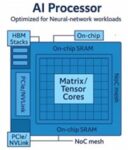
These developments dramatically increased the scale and complexity of SoC designs. AI-era chips routinely contain billions of gates, heterogeneous compute clusters, and sophisticated networks-on-chip (NOC) to move data efficiently between processing elements. See figure 1.
Figure 1: High-level block diagram of an AI processor.
In this context, HAV has taken on a fundamentally expanded role.
Verification is no longer confined to functional correctness in sub-billion-gate designs; it must now scale to multi-billion-gate systems and address far more than logic alone and even more than software stacks. Today’s HAV platforms are increasingly used to evaluate power and thermal behavior, analyze performance, validate safety and security requirements, capture full system-level interactions, and run realistic workloads that reflect how the design will operate in the real world.
At the same time, ICE-style operation matured into a critical engineering capability rather than a legacy mode. This is especially true in at-speed FPGA-based prototyping, where real physical interfaces must be validated at speed before committing a design to manufacturing. By allowing the design-under-test to interact with actual PHY hardware early in the cycle, ICE enables teams to uncover integration, timing, and signal integrity issues that purely virtual environments cannot expose. In doing so, it strengthens both hardware and software confidence long before tape-out.
Just as importantly, AI hardware cannot be separated from its software ecosystem. Compilers, runtimes, libraries, kernels, and deployment frameworks are no longer afterthoughts, they are inseparable from whether the hardware succeeds or fails. HAV platforms are therefore used to run real AI workloads well before silicon exists, ensuring that hardware and software evolve together rather than sequentially. The feedback loop between architecture and execution is increasingly closed before tape-out, not after first silicon.
In this sense, verification in the AI age has become truly full-stack. HAV is no longer just a tool for validation, it is now the environment where hardware/software co-design converges, enabling what might be called a new paradigm: software-driven tape-out.
Conclusion: HAV as the Engine of Hardware–Software Convergence
After four decades of evolution, the semiconductor industry has come full circle. Hardware complexity initially drove the rise of emulation as a practical necessity. The software era that followed expanded HAV’s role, connecting it to virtual environments, richer software stacks, and broader system-level workflows. Today, the AI revolution is once again reshaping the landscape, restoring hardware to the center of innovation and demanding unprecedented levels of specialization, efficiency, and scale.
What has changed most fundamentally, however, is the meaning of that centrality. Hardware is no longer designed first and programmed later. The defining trend of this decade is software-defined design, where architecture is shaped as much by compilers, runtimes, and workloads as by transistors, interconnects, and logic structures. The boundary between hardware and software has blurred into a single, tightly coupled engineering problem.
HAV platforms sit precisely at this intersection. They can no longer be viewed as tools for checking correctness in isolation. Instead, they have become essential environments for validating architectural intent—where hardware meets real software, where performance assumptions are tested under realistic workloads, and where system-level trade-offs are exposed while meaningful design changes are still possible. In the era of software-driven tape-out, HAV is the mechanism that closes the loop before silicon exists.
Hardware is once again the center of the universe, not because software has become less important, but because software has become so important that it now defines the hardware itself.
The metrics of success have shifted accordingly. Choosing an HAV platform is no longer simply a matter of how many gates can be verified for functional correctness. It is now about whether the full spectrum of software-driven use cases can be executed, analyzed, and optimized before tape-out. In this new era, hardware is not just the foundation beneath softwa2026 Outlook with Abhijeet Chakraborty VP, R&D Engineering at Synopsysre innovation, it has become one of its primary engines.
Easy-Logic Technology Ltd. is a specialized Electronic Design Automation (EDA) company focused on solving one of the most complex and time-sensitive challenges in semiconductor design: functional Engineering Change Orders (ECOs). Founded in 2014 and headquartered in Hong Kong, the company has built its reputation around advanced logic optimization algorithms that help ASIC and SoC design teams implement late-stage design changes quickly and safely.
In modern chip development, errors or specification changes often surface late in the design cycle, sometimes after synthesis, place-and-route, or even physical layout. At that stage, making changes manually can be extremely risky and costly. A single modification may ripple through large portions of the logic, potentially affecting timing, testability, or power consumption. Traditionally, engineering teams would rely on manual patching or partial redesign, which can extend schedules and increase the chance of introducing new bugs.
Easy-Logic’s core focus is automating this ECO process. Its flagship solution, commonly referred to as EasylogicECO, provides functional ECO automation that generates optimized logic patches directly from specification changes or RTL updates. Instead of requiring a full re-synthesis or broad structural modifications, the tool computes minimal patch logic that satisfies the new functionality while preserving as much of the existing netlist as possible. This significantly reduces disruption to timing closure and layout integrity.
One of the key strengths of Easy-Logic’s approach lies in its algorithmic foundation. The company was founded by researchers and engineers with strong academic backgrounds in logic synthesis, formal methods, and verification. By combining formal equivalence techniques with optimization strategies, the tool can identify the smallest set of logic changes needed to meet new design requirements. This minimizes area overhead and maintains design stability, critical factors in advanced process nodes where margins are tight.
Another important area of capability is post-layout ECO support. In late tape-out stages, designers often prefer “metal-only” ECOs, where changes are implemented by modifying metal layers without altering lower layers of the silicon. This approach reduces manufacturing costs and avoids restarting expensive mask processes. Easy-Logic’s solutions are designed to support these constraints, enabling functional updates while preserving physical design structures. This makes the tool particularly valuable for high-volume ASIC programs with strict deadlines.
Scan chain repair and DFT preservation are also integrated into the ECO flow. Functional modifications can disrupt scan connectivity, which is essential for manufacturing test coverage. Easy-Logic addresses this by automatically repairing or maintaining scan chains after logic patches are applied. This ensures that testability remains intact without requiring separate manual correction steps.
Within the broader EDA industry, Easy-Logic occupies a focused niche. The global EDA market is dominated by large vendors offering end-to-end tool suites covering synthesis, verification, simulation, and physical implementation. Rather than competing directly across all categories, Easy-Logic concentrates on the functional ECO segment. This specialization allows it to deliver deep technical solutions in an area that is critical but often underserved by broader platforms.
The company’s tools are used by semiconductor firms developing complex ASICs for consumer electronics, networking, artificial intelligence accelerators, and industrial applications. As chip complexity increases with billions of transistors integrated into advanced nodes the likelihood of late-stage design changes grows. ECO automation therefore becomes increasingly important for meeting aggressive time-to-market targets.
Beyond time savings, Easy-Logic’s solutions contribute to risk reduction. Late design changes are inherently dangerous because they can unintentionally impact previously verified functionality. Automated formal verification embedded within the ECO flow helps ensure that only the intended modifications are introduced. This reduces the probability of silicon re-spins, which can cost millions of dollars and months of delay.
Bottom line: Easy-Logic Technology Ltd. represents a highly specialized player within the semiconductor software ecosystem. By focusing on functional ECO automation, it addresses a bottleneck that directly affects schedule, cost, and design stability. As semiconductor projects continue to grow in complexity and competitive pressure increases, the ability to implement safe, minimal, and efficient late-stage logic changes will remain a critical advantage and that is precisely the domain in which Easy-Logic has built its expertise.
The Electronic System Design Alliance (ESDA) has been at the center of the EDA industry through its many changes over the years. It occurred to me that an update on this organization would be useful. ESDA is a technology community within SEMI and is managed primarily by a team of three who coordinate all its activities along with a group of dedicated volunteers from member companies. I had the good fortune to spend some time with two of those core team members recently.
We had a great time talking about the phases of ESDA’s story and the achievements that were made along the way. I realized this story needed telling. Those EDA veterans among us will know some, but maybe not all of it. And those who are new to EDA should know how the industry got here. The story has many twists and turns, but one simple fact rang out during our discussion about ESDA. The name changes but the vision remains the same. Let’s look at ESD Alliance through the years.
Who’s Talking?
Bob Smith
The two gentlemen I spoke with were Bob Smith, Executive Director of ESD Alliance and Paul Cohen, Sr. Manager ESDA & R&D. I’ve known both Bob and Paul for a long time and I’ve had the pleasure of attending many of their events. I even helped to create a few of them. As we go through the story I’ll add some of my experiences as well. A couple of quick bios are appropriate:
Before ESDA, Bob was senior vice president of marketing and business development at Uniquify. Bob began his career as an analog design engineer working at Hewlett Packard. Since then, he has spent more than 30 years in various marketing, business development and executive management roles primarily working with startups and early-stage companies. These companies include IKOS Systems, Synopsys, LogicVision, and Magma Design Automation. He was a member of the IPO teams that took Synopsys public in 1992 and Magma public in 2001.
Paul Cohen
Paul Cohen has been with the various incarnations of ESDA for over 18 years. He is indeed the class historian. Prior to ESDA, Paul had a long career in semiconductor design/applications and EDA at companies such as Virage Logic, Fujitsu Microelectronics, Design Acceleration Inc, IDT, Prime Computer, and Digital Equipment Corporation. Paul began his career at General Electric.
The Beginning – EDAC
The story begins in 1989 when a group of EDA companies formed the group, Electronic Design Automation Companies, EDAC, to negotiate with the increasingly important trade show portion of the Design Automation Conference. DAC had been a prestigious technical conference for many years, dating all the way back to 1964. Momentum for commercial exhibits at the event began in the mid-1970s, and by the early 1980s, the trade show became a core element. The first commercial DAC was held in June 1984.
The EDA Companies became the EDA Consortium in 1996, continuing its role working with DAC while addressing additional industry-wide issues. The organization incorporated and became a co-sponsor of DAC in 1992, alongside the IEEE and ACM.
Many other important events occurred during this time that shaped the future of the EDA industry. One was the establishment of the Phil Kaufman Award, the highest recognition in the EDA industry. A Nobel Prize for EDA of sorts. The award took its name from Phil Kaufman, a pioneer in EDA who passed away in 1992. The IEEE Council on Electronic Design Automation (CEDA) became a co-sponsor in 2005.
The first Kaufman award was given to Dr. Hermann Gummel in 1994. Gummel was a researcher at AT&T Bell Laboratories. He was recognized for his many fundamental contributions to central areas in EDA, including the integral charge control model for bipolar junction transistors that bears his name, the Gummel-Poon model. I knew both Hermann Gummel and Sam Poon – incredibly smart people.
Over the years, the coveted Kaufman Award has recognized some truly great pioneers. You should check out the all-star list here.
In 2021, ESDA and CEDA created the Phil Kaufman Hall of Fame to posthumously recognize individuals who made significant contributions through creativity, entrepreneurism and innovation to the electronic system design industry and were not recipients of the Phil Kaufman Award.
Jim Hogan, executive, angel investor and board member, and Stanford University Professor Edward J. McCluskey were the first honorees.
In 1994, EDAC published the first Market Statistics Service (MSS) report (now the Electronic Design Market Data – EDMD – report). The report included detailed revenue that was reported in confidence by public and private EDA, IP, and services companies, allowing companies, investors and analysts to track trends in the industry. Over the years, these reports have tracked the substantial growth of the EDA industry. Walden C. Rhines is the Executive Sponsor of the SEMI Electronic Design Market Data report and has been from the start. You can hear the latest results of these reports on the Semiconductor Insiders Podcast Series on SemiWiki. Here is the most current report.
Also, during this first phase in 2009 the organization coined the term EDA, Where Electronics Begins. You can see the associated logo at the top of this post. The catch phrase was accompanied by an informative video. The forward-looking vision conveyed by this work has stood the test of time. Today, it’s as relevant as ever and the organization continues to promote these ideas. This enduring vision was the catalyst for this post’s title. It essentially named itself.
I will offer one more story from this era. In 2013, EDAC put together a substantial fund-raising event called EDA: Back to the Future. It was billed as an “industry reunion”, but the primary focus was fund raising to ensure EDA had its proper place in history. The event was held at the Computer History Museum in Mountain View.
I was one of several folks who worked on the production of the event. There was a live auction and a silent auction, and a significant amount of money was raised to help document EDA’s contributions to the development of computing technology.
One last piece to share on this one. I was at eSilicon at the time, and we were the sponsor of an American Le Mans racing team called The Flying Lizards. We donated a ViP pit crew pass for the upcoming race at Laguna Seca for the live auction. Someone everyone knows at SemiWiki was the proud winner of that auction lot, Dan Nenni.
Expanding the Footprint – ESDA
In 2016, The Electronic Design Automation Consortium became the Electronic System Design Alliance. This name change supported a significant shift in the EDA industry. EDA tools were now being used for more than just chip design. The realization was occurring that collections of chips were becoming the backbone of new systems, and the need to expand EDA technology into that realm became important.
We saw a gradual shift in focus that went beyond the boundary of a single piece of silicon. EDA was becoming more widespread, and this spawned another wave of growth. Electronic system-level design became a thing.
Beyond this shift in design focus, there was another fundamental change occurring. EDA was no longer just about design tools. Semiconductor IP was gaining significant momentum as an enabler to build new systems more quickly and reliably. During our discussion, Bob Smith described an encounter at a Board Meeting with Simon Seagers. Simon was the CEO of Arm at the time and a member of the Board. Simon was lamenting the fact that he was part of an electronic design automation consortium, but he didn’t provide EDA tools.
IP was quickly becoming a substantial piece of the EDA market. Bob explained that Simon’s comments were taken seriously and that helped to move the organization toward a new and broader identity.
A Seat at a Bigger Table – SEMI
In 2018, the ESD Alliance became a SEMI technology community. The organization was now part of a global entity that brings together more than 3,500 member companies to make a difference on top industry issues for the microelectronics industry. Bob Smith described this phase as “the changing of the guard”.
Back to that enduring tagline, EDA, Where Electronics Begins. The team that invented that vision is now part of a substantial organization that is helping the larger audience of EDA users. On the surface, this seems like a perfect fit. In my conversation with Bob and Paul, I discovered something that is obvious if you think about it a bit.
Change is difficult and takes time. As part of the shift to SEMI, ESDA began to co-locate chip design events with the popular SEMICON expositions that SEMI held. This seems perfect – one event where the entire spectrum of design and manufacturing for semiconductors could be explored.
What Bob and Paul observed in the early days of these co-located events was very little “cross-over” behavior. Those who focused on manufacturing went to that part of SEMICON and those that focused on design went to ESDA’s event. This fact reflects the significant shift that is still occurring today to bring design and manufacturing together into one focus. Complex system designs, fueled by AI workload demands is driving it. So is heterogeneous multi-chip design. This discipline is driven significantly by material innovation in packaging, which is tied closely to manufacturing.
Bob and Paul also shared that they are seeing a shift in behavior at more recent SEMICON events. That integration of design and manufacturing focus is starting to happen. Welcome to the new world of semiconductors.
Some Final Thoughts
I have just scratched the surface of the impact from the organization formerly known as EDAC. There is so much more to the story, and we will dig deeper in future posts. Before closing, I want to thank Bob and Paul for spending time with me. And thanks to Nanette Collins for making it happen.
I got to know both Bob and Paul a bit better during our conversation. It’s worth mentioning there are other, non-EDA sides to each of these folks. Bob Smith is also a co-founder of a winery called Jazz Cellars, located in Murphys, CA. I have fond memories of attending EDAC and ESDA events where Bob would pour wine from Jazz Cellars.
Paul is something of a photography geek. He wields equipment far more sophisticated than the latest iPhone with great results. These skills have been quite valuable over the years to chronicle all the terrific events that the organization has delivered.
If you’d like to learn more about ESDA and its role in SEMI, this is a good place to start. And that’s how the name changes but the vision remains the same.
In the modern world, the semiconductor industry stands at the heart of technological innovation. From smartphones and laptops to advanced medical devices and artificial intelligence systems, nearly every piece of contemporary electronics depends on increasingly sophisticated microchips. Among the leading companies driving this progress is Taiwan Semiconductor Manufacturing Co., Ltd. (TSMC), the world’s largest pure-play semiconductor foundry. Through continuous research, advanced manufacturing techniques, and aggressive scaling strategies, TSMC has played a pivotal role in pushing the boundaries of what is possible in chip fabrication.
As semiconductor technology advances, one of the most critical goals is scaling down device dimensions. Smaller transistors allow for higher device density, faster switching speeds, and lower power consumption. However, shrinking dimensions introduces immense engineering challenges. At technology nodes such as 5nm and beyond, even minute variations in patterning can significantly impact device performance and yield. Achieving precise control over distances between features, such as the “end-to-end” spacing between adjacent structures, becomes increasingly difficult as these distances approach tens of nanometers.
Traditional lithographic processes often require multiple patterning and etching steps to achieve extremely tight spacing. In earlier approaches, forming patterns with very small end-to-end distances might involve three separate lithography steps combined with multiple etching stages. Each additional step increases production time, cost, and the potential for alignment errors. Overlay inaccuracies between masks can lead to critical dimension variations, negatively affecting device reliability and manufacturing yield. Therefore, reducing the number of processing steps while maintaining or improving precision is a key objective in advanced semiconductor fabrication.
One important innovation involves using a single lithographic process combined with carefully engineered etching techniques to achieve sub-35 nm end-to-end distances. Instead of relying on multiple pattern transfers, this approach begins with forming unidirectional features in a photoresist layer using advanced lithography, such as EUV lithography. EUV uses very short wavelengths of light to define smaller features than previously possible with deep ultraviolet systems. By carefully designing the initial pattern and then applying a controlled angled etch process, the effective length of features can be modified without changing their width.
The angled etch technique is particularly significant. By directing ion beams at specific angles relative to the substrate surface, engineers can selectively trim or extend certain dimensions of patterned structures. For example, the length of a feature along one direction can be increased, thereby reducing the end-to-end spacing between neighboring features. This allows a final pattern to achieve tighter spacing than originally defined in the photolithography mask. Importantly, this method maintains the critical width dimension while adjusting only the desired axis, enabling precise dimensional control.
Such process optimization provides several advantages. First, it reduces the number of required lithography steps from three to one, cutting down cycle time and manufacturing costs. Lithography is one of the most expensive and time-consuming steps in semiconductor fabrication, so eliminating even a single lithography stage can yield substantial economic benefits. Second, fewer process steps reduce the risk of cumulative defects and misalignment errors, improving overall yield and device reliability. Third, streamlined processing enhances throughput in high-volume manufacturing environments, enabling faster delivery of advanced chips to market.
In devices such as FinFETs, which are widely used at advanced nodes, precise pattern control is especially crucial. FinFET architectures rely on three-dimensional channel structures that improve electrostatic control compared to planar transistors. However, their 3D geometry increases fabrication complexity. Maintaining consistent spacing between contacts, gates, and interconnects ensures proper electrical isolation and performance. Techniques that achieve tighter end-to-end distances without increasing process complexity directly support the continued scaling of FinFET and future transistor architectures.
Ultimately, innovation in semiconductor manufacturing is not just about making features smaller; it is about doing so efficiently, reliably, and economically. Companies like TSMC continue to invest heavily in process integration, materials engineering, and advanced patterning technologies to sustain progress beyond the 5nm node. By combining advanced lithography with creative etching strategies, the industry can overcome scaling barriers that once seemed insurmountable.
Bottom Line: As global demand for computing power grows driven by artificial intelligence, 5G communications, autonomous vehicles, and high-performance computing, the importance of such innovations will only increase. The ability to control nanometer-scale distances with extreme precision represents not just a technical achievement, but a foundational capability that shapes the future of modern technology.
Juniyali Nauriyal is the CEO and Co-Founder of Photonect, a photonics startup focused on commercializing advanced fiber-to-chip attachment technologies. Juniyali is the co-inventor of Photonect’s core technology, which forms the foundation of the company. As CEO, she leads Photonect in translating cutting-edge photonic packaging research into scalable, real-world solutions.
She has participated in prestigious accelerator programs including Activate, the Luminate Accelerator. Under her leadership, Photonect won the Grand Prize at the New York State Business Plan Competition (2022). Juniyali has received multiple competitive awards and scholarships, including the Corning Women in Optical Communications Scholarship (2022) from Optica, the SPIE Optics and Photonics Education Scholarship (2022), the Harvey M. Pollicove Memorial Scholarship (2018) from Optica, and the Best ISA Student Award (2016) from ISA–Maharashtra. She currently serves as Vice Chair of IEEE Women in Engineering (WIE) Rochester and was named Emerging Technology Woman of the Year (2025). Juniyali holds 7 patents and has authored 20 technical publications, including 2 first-author papers.
Tell us about your company?
Photonect is a Rochester-based startup addressing a critical bottleneck in photonic packaging: slow, costly, and unreliable fiber-to-chip attachment driven by epoxy. Attaching an optical fiber is as delicate as aligning two strands of hair, yet current approaches rely on glue. Photonect’s technology includes a patented chip architecture design called the oxide mode converter and laser fusion process that forms permanent glass-to-glass bonds in under a minute. This improves coupling efficiency from ~50% to ~80%, maintains <1 dB loss, increases throughput by 10×, and reduces per-device cost by 50%. This technology is being advanced into PIX-Attach, a Rochester-designed laser splicing system built for high-volume photonic integration set to launch at OFC 2026.
Please share a little bit more about how company was founded?
Photonect was founded by Dr. Juniyali Nauriyal as a spin-off from the University of Rochester, rooted directly in her doctoral research in integrated photonics. Originally an engineering student in India, Juniyali came to the U.S. to pursue an MS in Optics at the University of Rochester, where she joined the lab of Dr. Jaime Cárdenas. That collaboration evolved into her PhD work and eventually started Photonect itself.
During her PhD, Juniyali co-invented Photonect’s core technology along with Dr. Cárdenas, who is now the company’s CTO and Co-Founder. Rather than taking a traditional path into a large tech firm, Juniyali chose to commercialize her research to ensure it could deliver real-world impact. Her work led to a breakthrough approach to fiber-to-chip light coupling, improving efficiency while addressing the growing sustainability challenges driven by AI and data-center expansion.
Inspired by issues such as the rising energy demands of data centers and even their migration to colder regions to manage heat, Juniyali founded Photonect with a clear mission: to build high-performance photonic technologies that scale responsibly and support a more energy-efficient future.
What problems are you solving?
We address the limitations of epoxy-based fiber-to-chip attachment, which is slow, costly, and inherently unreliable. Today, epoxy is commonly used to connect/attach optical fibers to chips even though these joints are critical to data transfer efficiency, often resulting in up to 50% signal loss, increased heat generation, and long, labor-intensive assembly times that severely limit scalability. Our laser-assisted attachment technology replaces epoxy with a glass-to-glass bond, like soldering. This enables fiber-to-chip attachment in seconds instead of minutes, while delivering long-term reliability and stability across wide temperature ranges. In parallel, our proprietary mode converter technology significantly improves coupling efficiency, achieving <1 dB loss per chip facet and reducing overall link budget requirements by ~25%.
What Industries is your solution a good fit for ?
Our solution is a strong fit for industries undergoing a shift toward dense, high-performance optical integration, driven by the speed, power, and reliability demands of modern computing. This includes AI data centers and cloud infrastructure, high-performance computing, telecommunications, and emerging markets like quantum technologies. As copper and conventional photonic interconnects hit physical limits, Photonect’s technology delivers a step-change in performance, scalability, and energy efficiency, enabling these industries to keep pace with rapidly growing system demands.
What keeps your customers up at night?
Our customers worry about scaling photonic products to high volume without blowing up cost, power use, or yield. Today’s fiber-to-chip attachment is slow, energy-intensive, and requires specialized manpower, often forcing teams to choose between scalability and efficiency putting timelines, margins, and reliability at risk specially now as AI and data-center demand accelerates.
Q6.What does the competitive landscape look like and how do you differentiate?
In fiber-to-chip attachment landscape, existing solutions include wire bonding, fiber packaging with epoxy, and passive alignment approaches some players offer high-precision automated assembly systems that still rely on active alignment and adhesive bonding, none of which have been able to fully replace epoxy. Photonect takes a fundamentally different approach by adhesives through its proprietary laser-assisted attachment process. Our technology enables fiber-to-chip attachment in few seconds, achieves <1 dB optical loss, and delivers throughput of up to 60 attachments per hour.
In addition, our proprietary mode converter designs further reduce coupling losses by 15–20%, while maintaining high power compatibility and reliability across extreme temperature ranges.
What new features/technology are you working on?
We’re working on PIX-Attach, a next-generation laser-assisted, epoxy-free fiber-to-chip attachment platform that dramatically speeds up photonic packaging, cutting attach time to ~60 seconds per unit, enabling ~60 units per hour, improving alignment stability, reducing energy use, and significantly increasing production throughput while lowering the number of machines needed on the factory floor. Our value proposition lies in creating a premium and customized fiber attach equipment that fit’s the customers need. We are all set to launch this in mid-March 2026.
How do customers normally engage with your company?
We’re present at all major conferences such as OFC, Photonics West, and ECOC. You can also reach out to us directly at info@photonectcorp.com, or submit a query or request a meeting through our website.
Daniel is joined by Linley Gwennap, technology analyst and author of the new book “How AI Really Works: The Models, Chips, and Companies Powering a Revolution.” Linley was the long-time editor of Microprocessor Report and chaired the popular Linley Processor Conferences.
Dan explores what impact AI is having on the market and the population with Linley, who offers some straight-forward explanations of how AI is impacting our world. Trends in AI model size are discussed, as well as competitive dynamics. Linley offers perspectives on how trends today and in the future will impact the market size and the key players. Trends in AI model size are also reviewed, along with some predictions about how AI will impact the overall workforce, both now and in the future.
The views, thoughts, and opinions expressed in these podcasts belong solely to the speaker, and not to the speaker’s employer, organization, committee or any other group or individual.
Chip design is getting more difficult as technology advances. Everyone knows that. A lot of the discussion around these issues tends to focus on the demands posed by massive AI workloads and the challenges of shifting to heterogeneous multi-die design. While these create real problems, there is an underlying effect that is making the situation much worse than it needs to be: The ROI on advanced-node scaling is compressing in ways most teams do not yet quantify.
For three decades, Moore’s Law was an economic engine. Today, at 3nm and below, that engine is slowing. While foundries promise massive PPA (power, performance, and area) gains, the reality for most design teams is a “Performance Mirage.” Despite multi-billion-dollar investments in 3nm Gate-All-Around (GAA) and FinFET migrations, a large portion of the promised performance of these advances can be out of reach. It is often being sacrificed to “margin” reserved solely to compensate for modeling uncertainty. Let’s refer to this structural inflation of clock margin as the “Pessimism Wall”.
The good news is that this margin is not a law of physics. It can be safely reclaimed and redirected toward real silicon limits. More on that shortly. But first let’s answer the question, what is the 3nm pessimism wall and why is it an economic crisis? The answer begins with understanding how margin accumulates – and why that accumulation has become economically consequential.
Anatomy of the Crisis
At 3nm, clock sign-off guard bands have exploded to 25–35% of the total clock period. This is not a choice; it is a structural consequence of abstraction-based sign-off methodologies. The following data highlights the mechanisms driving this structural margin inflation.
The data below reflects trends widely observed across advanced-node programs. While exact values vary by design, the structural pattern is consistent.
The 2.5x Over-Design Trap: Applying 28nm-era sign-off assumptions to 3nm designs forces designers to over-design clock networks by 2.5x. You are often paying for buffers, area, and routing complexity that the silicon does not need.
The Near-Threshold Danger Zone: As voltages approach device thresholds, delay behavior becomes exponential and non-linear. Standard static timing analysis (STA) over-linearizes these effects, forcing an “uncertainty tax” of 8–12% of the clock period just to remain “safe”.
The Jitter Black Hole: Power-supply-induced jitter (PSIJ) and simultaneous switching now consume 5–10% of the margin. Traditional tools treat this as a static guess.
All these effects hide useful margin behind the pessimism wall.
A Closer Look at the Pessimism Wall
Every picosecond of unnecessary margin has a direct impact on the project’s bottom line. The following table breaks down the contributors that can cumulatively drive total clock margin toward ~25–35% range:
The contributors above are individually defensible and grounded in advanced-node physics. What creates the pessimism wall is their cumulative stacking.
In abstraction-based sign-off flows, voltage sensitivity, jitter, aging, and variability are typically evaluated independently and conservatively. Worst-case assumptions stack because electrical interactions are not jointly resolved in time and voltage.
The silicon did not become 35% worse. Our abstractions became cumulatively more conservative. To be clear, the issue is not transistor device models themselves. The structural pessimism arises from abstraction-based timing methodologies and independently stacked worst-case assumptions that approximate electrical behavior rather than directly solving it.
The Economic Consequences – A Crisis in the Making
Leaving 10–15% recoverable clock margin on the table is not a modeling inconvenience – it can be a massive competitive liability. Let’s look a bit closer at what’s involved.
The Power Penalty: Because dynamic power scales with the square of voltage, a 10% reduction in margin translates to a ~18–20% reduction in dynamic clock power. Given that clock networks consume 30–40% of SoC power, this often determines whether a design leads its segment or thermally limits its own performance.
The Revenue Loss (SKU binning): Reclaiming ~10% margin enables a 300 MHz boost on a 3 GHz target. In high-volume production, shifting even 10% of volume into a premium performance bin can represent hundreds of millions of dollars in incremental revenue currently sacrificed to uncertainty.
Area Inefficiency: Abstraction-driven margin forces aggressive cell upsizing, leading to a 10–15% increase in clock tree area. This bloats die size and increases per-unit cost across millions of chips.
Field Failures: The industry’s reliance on broad “Guard Bands” actually increases risk: – Masked Failures – Broad margins “hide” specific electrical failures—like rail-to-rail or duty-cycle issues – until they hit the field. – Aging Roulette – Applying “Global Aging Taxes” ignores path-specific stress, leading to chips that pass tapeout but degrade prematurely in the field.
The Solution: Full-Clock Physics Enforcement
The crisis stems from one fact: Models have stopped keeping up with physics.
The most direct way to address structural pessimism is to replace timing abstractions and estimates with electrical resolution by performing detailed, accurate SPICE analysis on the entire clock. Up to now, this wasn’t practical for two reasons. First, standard SPICE runs on networks of this size would take an unreasonable amount of time and consume vast (and expensive) compute resources. And second, standard SPICE can’t even load networks of this size.
The good news is that these barriers are now gone. The ClockEdge Veridian suite delivers a family of SPICE-accurate analysis engines for timing, power, jitter, and aging. And Veridian delivers sign-off precision at real-world speed, revealing interactions that conventional flows miss. This enables full-clock waveform fidelity across timing, power, jitter, and aging interactions.
Veridian engines enable billion-transistor, unreduced SPICE analysis performed overnight. Some of the benefits of this include:
Eliminate Abstraction-Driven Guesswork: Enforce Kirchhoff’s Current and Voltage Laws across the entire netlist to eliminate table-lookup errors
Expose Hidden Failures: Veridian identifies rail-to-rail and duty-cycle failures that traditional STA “masks” with margin until it is too late
Path-Specific Aging: Stop applying global derates. Measure actual aged behavior to recover margin safely
The question is no longer whether the pessimism wall exists – physics proves it does. The question is whether your methodology is capable of exposing it before your competitor does.
At advanced nodes, competitiveness is increasingly determined not by how much margin can be added, but by how much unnecessary margin can be safely removed.
The 3nm Pessimism Wall is not a silicon limitation – it is a modeling one.
The teams that resolve physics directly rather than approximate it will reclaim performance, power efficiency, and yield that others continue to surrender to uncertainty.
To Learn More
ClockEdge recently published a very informative white paper titled Reclaiming Margin in Advanced Nodes – Why Abstraction-Based Sign-Off Is Becoming the Dominant PPA Limiter at 3nm and Below.
This white paper is essentially a master class in how to preserve margin, performance and profits at advanced nodes. If you find yourself becoming a “slave” to ever-increasing design margins, this white paper is must-read. You can access your copy here. And that’s what the 3nm pessimism wall is and why it is an economic crisis.