One of the present ironies of the Internet of Things is as it seeks to connect every device on the planet, we are still designing those things with largely unconnected EDA tools. We may share libraries and source files on a server somewhere, but that is just the beginning of connection.
It is not surprising that synthesis tools from Altera, Xilinx and other FPGA vendors are vastly different in terms of where they put files and how they are configured. This becomes painfully evident to design teams as soon as they try to target FPGAs from two or more vendors. IP written in RTL that is theoretically “portable” and “synthesizable” can become lost in a forest of files, and have build and simulation settings applied that shake unexpected errors loose.
A team working with one FPGA architecture may have become used to the idiosyncrasies of that tool set. New designers, even those familiar with the synthesis and simulation tool itself, may find a steep learning curve in the details of reviewing designs and getting known-good IP to work. In many cases, the learning from the learning curve isn’t written down anywhere.
The problem is magnified when teams are distributed, with differences of distance, time, and language. The old adage “it takes longer to show someone how to do it than it does to actually do it” comes into play, which is a drag on productivity and a deterrent to scalability. Design teams know they have to share files, but often miss sharing the configuration details.
As FPGA designs have gotten larger and more numerous, and expertise comes from all over the globe, the problem is getting more urgent. Aldec and Synopsys each have vendor-independent FPGA synthesis and simulation tools, but Aldec is taking the next step in distributed team-based design management with their new release. I had a few minutes with Satyam Jani, product manager for Aldec Active-HDL, for some insight on what drove the latest improvements.
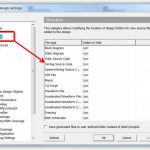
Based on feedback from actual users, the latest Active-HDL 9.3 release supports a user-defined folder structure. This ensures that designers have a consistent methodology in placing files, and prevents the problem of IP getting lost amongst the trees – especially when IP needs to be retargeted, alleviating the need to relocate files to match the other tool. It also facilities the design review process, because teams customize the structure to meet their needs exactly and know where to look for what types of information.
Part of that customized structure is a mix of file types: HDL files, schematics, text, waveform, and scripts. When the project with the HDL files are loaded, startup scripts can be executed to set the working directory, initialize local variables, set debug preferences, set the underlying standard level (for instance, VHDL 2008 or VHDL 2002), and other parameters. This allows teams to establish build consistency automatically, without written cookbooks a designer has to follow and the possibility (probability?) that different team members take different steps.
Also handy is the team category applied with an .adf file, which controls simulation. At different stages, designs are put through different tasks. For instance, initially a waveform viewer may be utilized. When issues are found, a debugger is brought in to isolate the problems, and finally a code coverage tool is applied. Each of these modes usually requires the simulator to be reconfigured manually, but with the team category the desired settings are defined and available in a pull-down menu, capturing the learning curve for everyone to use.
There are several other minor changes in this Active-HDL release. One I find fascinating is the ability to place JPG, PNG, and BMP files on a schematic. This has two uses: watermarking a design with a logo, and annotating a design visually to indicate a point of emphasis. The waveform viewer has also been enhanced, with saved settings and new comparison files, and support for floating point values. These and several other enhancements came directly from user inputs on making the tool more connected.
Aldec Active-HDL FPGA Design Creation and Simulation
I’m totally convinced that the path forward for technology innovation in the near term is not in creating yet-another-standard seeking to disrupt the norm, but instead including things in a framework that allow various approaches to work together. That is not an easy task, but it has tremendous value, and I think the folks at Aldec are doing a remarkable job of creative inclusion.
More articles by Don Dingee…
lang: en_US