In today’s world of semiconductor design with SoCs having complex IPs, hardware and software working together on a single chip, it’s hard to imagine a system without embedded software into it. But it is easy to guess how difficult it would be to test that hardware and software embedded system. And often there is limited window of time to test that complex system. If I recollect from my initial days of software development when I used to test every function, bottom up by using printf() statements, it is unimaginable that testing these systems will ever complete. Today, on-chip debug logic is being put on the embedded processor and testing is done smartly in real time, on-the-fly.
On-chip debug logic does allow run-control way of debugging by setting breakpoints, but that approach is intrusive and stops the system at those points to examine its state. This approach is okay for small simple systems, but is not suitable for complex multi-processing system and system which require the embedded processor to continuously run, control the feedback loops and maintain mechanical stability. It cannot detect problems at full clock speed and provides limited insight into asynchronous interrupt handlers.
The other approach of on-chip debugging is by utilizing ‘real-time trace’ mechanism which is much advanced and non-intrusive. Cycle-accurate timing information about the program execution, data access and details about surroundings (forward and backward) of specific events can be obtained with single or multiple cores running together. This approach has proved significantly important and widely accepted in safety and performance critical applications such as aerospace, automotive, medical, banking and mobile communications.
So, how does the ‘real-time trace’ work? Traces of all executed instructions by the processor in real-time are captured in a buffer (along with the data as required) to be analysed later. It’s possible to analyse trigger conditions as well. It provides deep insight into the system code without any effect on CPU performance and enables engineers to figure out what exactly brought the system to a state or conditions it is in.
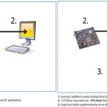
[Working of real-time trace with trace buffers]
Mentor Graphicsrecommends Vitra-XD trace probe developed by Ashling Microsystemsto be used for real-time trace debug. It is clear from the above picture that a combination of Mentor’s Sourcery CodeBench and Vitra-XD has made debugging pretty fast compared to a system with normal on-probe trace buffer with limited capacity. Vitra-XD provides a large buffer (supplemented by an on-device 500 GB hard drive) for storing a vast amount of trace data, thus increasing the probability of capturing and identifying most of the problems. It has 12.8 GB/sec 16 bit parallel trace data capture rate and a timestamp generator which can stamp the captured data at a resolution of 5ns.
As real-time trace is non-intrusive, it provides accurate timing information which helps in investigating timing bugs that may not be caught by other methods. Also, this method works exceptionally well to catch hard-to-detect intermittent problems or in cases where the system reaches unexpected faulty state. Similarly, it is handy to trace back from the point of data corruption or processor exception to analyse what exactly caused these to happen.
In modern world where most of the applications are becoming performance critical, it has become essential to use such debug systems in semiconductor design and SoC development. Most of the ARMprocessors include an embedded trace macro cell (ETM) for this purpose. Mentor Graphics and Ashling Microsystems have rightly identified this opportunity to provide a robust state-of-the-art system to trace, inspect and debug large amount of real time data. There is a whitepaperat Mentor’s website which provides a lot of details about real-time trace, how it works and several of its advantages. It’s worthwhile to read that and gain advantage!
More Articles by Pawan Fangaria…..
lang: en_US