Last week, after learning from the press releaseof Carbonabout its rocking sustained growth with record-breaking revenue and a thumping 46% increase in bookings, I was interested to know some more details about what drives Carbon to such an amazing performance in an EDA market that is generally prone to growth of a few percentage points provided the economic circumstances remain favourable. I was lucky talking to Bill Neifert of Carbon Design Systems who provided great insights into the value-added business model that is driving this kind of growth at Carbon and also about the ESL (Electronic System Level) segment. Here is the conversation –
Q: Bill, I know Carbon is among the very early movers into ESL area with its virtual prototyping product, SoC Designer. What are the various offerings you have that are gaining traction?
Carbon has been in the virtual prototyping space for nearly twelve years now, first with our Carbon Model Studio product and then with Carbon SoCDesigner. We rolled out Carbon IP Exchange a few years ago to meet the huge demand for automated model creation with an automated web portal. It’s really our CPAKs (Carbon Performance Analysis Kits) though which have been driving growth. While our other tool offerings are models and tools to create your own virtual prototypes, CPAKs are completely pre-built virtual prototypes and software which enable designers to be productive within minutes of download. If needed, they can then customize these very easily to more closely model the behaviour of their own system. We’ve found that by using CPAKs, we can enable users to be quickly productive across design tasks ranging from architecture analysis to system level performance optimization.
Q: I notice that you used the term virtual prototyping instead of ESL. What do you see as the difference?
ESL seems to mean something different to everyone. For some people it means high level synthesis (HLS). For others, it means a virtual prototype representation of the system. Another set of designers may use it to mean an architectural conception of the system as a starting point for successive refinement. Although I see lots of design teams using various parts of this definition, it’s pretty rare to see people using the entirety of design flows which can be lumped into the ESL term. We like to stick with using the term virtual prototype but even in that term there is some ambiguity since there can be virtual prototypes at differing levels of abstraction depending upon the models it contains. Our SoCDesigner-based virtual prototypes typically have multiple layers of abstraction depending upon the design need being addressed (ARM Fast Models for the software engineer, 100% accurate ARM models for the architect). Other virtual prototypes tend to stick to a single abstraction level and therefore, a single use case.
Q: Lately, I see that Carbon’s focus has been on providing complete solution for SoC designs, such as creation of accurate virtual models, Carbon IP Exchange through web based support etc. I would like to hear your comments on this.
Carbon IP Exchange is really software as a service (SaaS) application of Carbon Model Studio targeted for specific IP. For example, our relationship with ARM provides Carbon with access to ARM’s RTL to compile and instrument 100% accurate models based upon their IP.
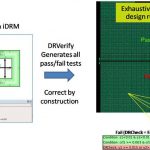
We rolled out the Carbon IP Exchange website to automate this model creation task. It walks the user through the configuration options for each piece of IP when each option is chosen. The form updates itself to allow only valid choices for each of the additional options. This way, when the form is complete it will correspond to a valid configuration for the RTL. The resultant model is therefore correct by construction based upon the configuration options supported in the RTL.
Along with the models, we also have a growing collection of Carbon Performance Analysis Kits (CPAKs). These CPAKs are pre-built virtual prototypes and system software. These CPAKs are user extensible and shipped with source code to enable simple customization.
Carbon IP Exchange is a vital part of our customer’s design infrastructure, it’s available 24/7 round the clock. It has already been used by designers to create over 5,000 models. This doesn’t include the several thousand additional models which are included in our CPAKs. This enables designers to be much more productive since they don’t worry about model creation. We enable them to be more productive by concentrating their efforts on doing actual design and debug, not worrying about the correctness of their model.
Q: How does web based Carbon IP Exchange work? Can any third party IP be modeled on-the-fly as per SoC design need? How about licensing?
Any third party IP could utilize Carbon IP Exchange. After all, we’re using the Carbon Model Studio compiler to generate the designs from the original RTL. That technology has been successfully used on projects for over a decade. We’ve tended to focus more on IP which our customers are using in their own SoC designs. This is why you see most of the top IP providers represented on the portal. We still of course also provide the Carbon Model Studio tool to design teams as well to enable them to compile models from their own RTL or from IP providers who aren’t currently on Carbon IP Exchange.
Q: I recollect from the press release that Carbon Performance Analysis Kits (CPAKs) are seeing rapid adoption by SoC design houses. How do they fit into the overall solution?
We rolled out CPAKs about 18 months ago and they are now in use at a majority of our customers. The reason for this is quite simple: they get designers up and running much more quickly. CPAKs are prebuilt virtual prototypes and software targeted at various use cases. The use cases vary. IP level optimization typically requires bare metal software for configuration and benchmarks. Driver development is generally done on a more complete system with a ported version of Linux or Android. Finally, a designer doing OS level performance optimization generally wants a complete system together with benchmarking applications. We have CPAKs targeted at each one of these use cases and package them together with source code for both the virtual prototype as well as the software which runs on top of them. This means that they can get you up and running quickly and also be easily modified to represent the actual configuration of your system. Using CPAKs it’s not unusual for a designer to be productive within minutes of download. It will take much longer, if they assemble that system themselves.
Q: My observation from our conversation is that it’s huge productivity gain for SoC designers, which is driving them to increasingly use Carbon’s solution or products for fast and accurate virtual prototyping that leads to silicon success in shorter time. Am I right in assuming that?
When you’re designing an SoC you typically have a bunch of questions: how fast will it run? What IP do I need? How much power will it consume? How do all the parts work together? Many more questions come to mind as well. The faster these questions can be answered, the sooner the project can be successful. The evolution of Carbon’s solutions is focused entirely on reducing the time needed to answer these design questions.
Q: O.K. looking at customers, I guess U.S. is always leading in newer as well as mature businesses. You say there is strong growth in Asia as well; can you elaborate a little bit on that? Is it because of many design and IP companies coming up in that region?
Virtual prototyping has always had a slightly different geographical sales mix than other EDA products. Japan was easily the strongest geography for many years but we’ve been seeing a dramatic shift in this in the past few years as the US takes on a more system-focused design flow and as companies in Korea, China and Taiwan do more and more designs. We grew so much last year by expanding dramatically in certain strategic accounts but also by acquiring accounts focused on additional vertical markets. ARM’s new 64 bit processors are being adopted by companies looking to build servers, storage and network devices. This is opening up a new set of customers to us as designers in those markets are adopting the same tools which have been used in the markets where ARM is already dominant.
Q: Would you like to further elaborate on continuing strategic partnership with Samsung and future roadmap?
Not yet, stay tuned!
Q: It’s interesting to know about such a progress happening in this space. One last question, what’s your view on ESL (i.e. use of virtual platforms, high level modeling etc.) entering into the mainstream of semiconductor design practices, at least for SoC designs?
I honestly believe that virtual prototyping is finally in the mainstream of the design practices for most SoC designs. I used to spend a lot of time talking to designers about why they should design using virtual prototypes. Now, that time is focused more on discussing the ways in which they can be using the virtual prototypes they have. Most design teams seem to be using virtual prototypes in at least part of their design flow. The key now is expanding that use throughout the entire flow to enable even greater value. EDA companies are successful when they remove design bottlenecks and CPAKs have demonstrated that they are able to get designers productive more quickly than with any other solution.
This was an interesting discussion with Bill. Now I can truly visualize how virtual prototyping adds value to an SoC design and how Carbon has made the process of virtual prototyping simple enough for it to get into the mainstream of semiconductor designs.
More Articles by Pawan Fangaria…..
lang: en_US