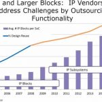
As your SoC design can contain hundreds of IP blocks, how do you verify that all of the IP blocks will still work together correctly once assembled? Well, you could run lots of functional verification at the full-chip level and hope for the best in terms of code coverage and expected behavior. You could buy an expensive emulator to accelerate your verification process. You could try an Assertion-Based Verification (ABV) methodology and learn to manually write assertions. Or, you could consider using a methodology for assertion reuse in SoC designs.
Two years ago I started hearing about Assertion Synthesis, the process by which assertions could be created for an IP block automatically instead of by hand-coding. It sounded interesting, and it turned out to be valuable enough that Atrentabought a smaller company called NextOp to acquire a tool called BugScope. Paul McLellan blogged about that acquisition here.
Ravindra Aneja talked with me this morning by WebEx and brought up this notion dubbed MARS – Methodology for Assertion Reuse in SoC. Design reuse is well-known and a widely accepted method to save time and improve quality, so why not assertion reuse? Here’s the promise of MARS then:
- It flags any IP that is incorrectly configured at the SoC level
- Any IP feature failure is flagged at the SoC level
- Any coverage targets missed by IP verification are pin-pointed
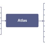
The whole idea is to provide a significant reduction in SoC Integration and debug time, while having a minimal impact on IP and SoC simulation run times. Plus, the MARS approach works with both emulation and FPGA-based verification environments. Here’s the proposed methodology flow:
A design or verification engineer would run BugScope on each IP block using functional tests and then look at the progressive test coverage report to understand:
- When to start generating assertions
- Are my IP tests mature enough yet
These automatically generated assertions are then ready to be re-used when the SoC has been assembled. Any violations of assertions would then be reported during SoC verification so that your team can fix SoC configuration bugs, fix specific IP design bugs, or fill in any IP coverage holes. Here’s an example of a progressive test coverage report:
This MARS approach is different than just ABV because BugScope is using the input tests to formulate the assertion automation. You can use assertion synthesis is you have ready access to the RTL code and tests for your internal IP, new IP, modified IP or even some 3rd party IP. Plan to target any control-intensive logic for generating properties: Arbitration, data flow control, interrupt controller, schedulers, etc.
Case Studies
The good news is that customers are using the MARS approach already, and in one case a customer had a critical IP block with about 1,400 tests defined. By using BugScope about 145 assertions were automatically generated, and when these assertions were re-used at the sub-system level there were 2 assertions fired. The first fired assertion uncovered an IP configuration error and the second fired assertion indicated that an important coverage hole was expected to be tested at the IP level.
In the second case a customer had some immature IP with a low verification confidence level, and BugScope generated 1,203 properties for re-use at the SoC level. With just 34 tests there were 105 properties fired, or about 10%. By looking through these properties they found that 48 unique and high priority IP coverage holes were exposed. The verification team now knew that their bus functional model needed to consider more realistic scenarios, that they needed to inject errors on multiple lanes simultaneously, and that clock skews was note test well enough at the IPO level.
Verification Management
To assist in the area of verification management there are three helpful feedback metrics:
- Verification and Testbench Grading – which tests are most effective
- Verification and Testbench Distribution – how exhaustive is each test, which coverage point needs more tests
- Verification and Testbench Balance – are there enough hits on my most complex modules
Summary
It is possible to accelerate SoC verification by finding IP configuration issues, IP design bugs and IP coverage holes. The Methodology for Assertion Reuse in SoC designs (MARS) is in use today. The BugScope tool from Atrenta also can cut time with emulation and FPGA-based debug approaches.
The evaluation process typically takes between one week to a month, based on your team size and schedule.
Marvel presented a paper at DAC in 2013 from Marvel about their experience with BugScope, and another customer has submitted a paper to DAC 2014.
lang: en_US