RVN! 26 Banner revised (800 x 100 px) (600 x 100 px)

EDAC Mixer: Sonoma Chicken Coop

EDAC Mixer: Sonoma Chicken Coop
by Paul McLellan on 04-02-2014 at 8:00 pm

Get together with your fellow industry peers and insiders at the monthly EDAC Mixer, to the benefit of local charities. You don’t need to donate anything, you just show up and pay for your own drinks. A portion of the proceeds will go to local charities, this month to the Resource Area for Teaching (RAFT), a San Jose based non-profit who’s main focus is to inspire, engage and educate children through the power of hands-on teaching. To learn more about RAFT, visit their web site here.

When is it? Thursday Thursday April 24th at the Sonoma Chicken Coop near San Jose Airport at 90 Skyport Drive, San Jose from 6pm to 8pm. That is right next to where Magma used to be (and just a 5 minute walk from the 1st Street light rail). There are other Sonoma Chicken Coops in San Jose, make sure you go to the right one! The menu has all sort of stuff but I strongly recommend the rotisserie chicken and the oven-roasted (is there any other way to roast?) vegetables. Full details here.

Although I doubt you will get thrown out if you just attend, EDAC would like you to register (it’s free) so they have some idea of numbers. Register here.

While talking about EDAC, yesterday the EDAC MSS released numbers for Q4 2013, up 5.7% compared to 2012 and up 8.7% compared to Q3. Full details in the press release here.

And another event to put on your calendar. The Emerging Companies Committee is sponsoring a new media panel. It will be held on April 17th at Cadence (presumably in the building 10 auditorium). Brian Fuller will moderate a panel with Sylvie Barak of Atmel, Hannah Conrad of Synopsys (who I’m guessing is the same person who used to be called Hannah Watanabe, congratulations), Benjamin Tompkins of Intel Free Press, and Lani Wong who just has to walk across the parking lot. There is a reception from 6-7pm and the panel will take place from 7-8.30pm. Full details here.

If you don’t want to go to that event, also on April 17th is the Electronic Design Process Symposium (EDPS) down in Monterey. Among other things that day you can hear me talk about FD-SOI, an under-rated technology that is swamped by all the talk about FinFET and about which you should learn more. Details here. Wally Rhines will be giving the dinner keynote at the Monterey Yacht Club. SemiWiki is a sponsor of the event.

UPDATE: Get $50 off EDPS for IEEE and non-IEEE regular tickets. Promo code: semiwikigo

So for the mixer, just in case it isn’t clear, here is what you do:
[LIST=1]

  • Decide to go
  • Register here
  • Show up at Sonoma Chicken Coop on Skyport at 6pm on 27th. Map.
  • Mingle with your industry colleagues
  • Pay for any food and drink you consume
  • Sonoma Chicken Coop will donate a percentage to RAFT

    More articles by Paul McLellan…


  • Sketch Router and auto-assist PCB layout

    Sketch Router and auto-assist PCB layout
    by Don Dingee on 03-31-2014 at 6:30 pm

    Archaic tech metaphors abound, stuck in the psyche of users everywhere. We still “dial” numbers, long after the benefit of a short pull area code disappeared. (Humans could dial 1, 2, or 3 a lot faster on a rotary phone, and there were fewer dialpulses for central office switches to decode – thus big cities with more phone traffic like New York, Chicago, and Los Angeles got their original area codes.) We press a small icon that looks like a floppy disk to save a document. We say “stay tuned” when there is more to a story coming soon.

    We have one of these terms in EDA: tapeout. That first job I mentioned in a recent post, designing and building analog autopilots? One sheet of translucent mylar per layer, black graphic tape, tape circles for through-hole pads, a lightbox, a ruler, an X-ACTO knife, and hours and hours under the tutelage of a very experienced and patient printed circuit board designer to create, check, and double check one board layout.

    Thank goodness that nonsense is over. In a modern PCB layout with 12 or 16 layers or more, surface mount packaging, fine pitch BGAs, controlled impedance, matched propagation delays, and dense routing tactics like blind and buried vias, automation is sorely needed – but not to be implicitly trusted. State of the art in PCB layout is moving to auto-assist, blending tool automation with designer experience so the layout is seen as it unfolds.


    Auto-assist is featured in the latest version of Mentor Graphics Xpedition, a PCB design platform targeting better productivity for complex designs. Xpedition represents an entire flow, from system definition, simulation, schematic entry, constraint definition, layout, verification, DFM, and design data packaging for handoff to fabrication. The focus is on reducing manual data manipulation and automating tedious tasks, a must for yielding successful layout faster, working within distributed teams and enabling effective reuse of layout IP quickly and accurately.

    There are many new features in Xpedition, and one of the more interesting is Sketch Router. Auto routing can produce some interesting (ok, bogus is more like it) results, especially on wide parallel bus structures, so designers usually resort to manual efforts to avoid problems in critical areas. Unfortunately, those are often the most crowded areas, requiring a lot of time and care.

    Sketch Router is an interactive auto-assist router providing more control and following intent, allowing guidance with simple, step-by-step visual feedback so the user can see exactly what is happening and adjust or retry as necessary. On the Sketch Router page, several short product demo videos show some of the capability.

    In difficult areas, hug routing creates local bias using existing routes as a guide to completing an area. Push and shove allows the designer to move traces around, automatically clearing planes as required. Groups of traces move smoothly, including curved trace routing for BGA patterns, and differential pair routing with phase matching. All this capability works with defined rules and constraints, helping to “paint” a layout to completion with better assurance of routing quality.

    Mentor has started a new blog series with Charles Pfeil and Vern Wnek, exploring the new capability in Xpedition and some real world PCB routing challenges. Both have put up their first entries in the Xpedition Enterprise Blog – it’s funny, Charles starts with a similar story to mine – and will be continuing the discussion there. There is also a webinar on Routing Automation with a longer presentation showing how Sketch Router works. If you’re interested in complex PCB layout issues, or trying to decide on an automation tool, these are good resources to explore.

    lang: en_US


    Sebastian Thrun: Self-driving cars, MOOCs, Google Glass and more

    Sebastian Thrun: Self-driving cars, MOOCs, Google Glass and more
    by Paul McLellan on 03-31-2014 at 4:00 pm

    Sebastian Thrun gave a fascinating keynote at SNUG last week. It didn’t have that much to do with IC design but he discussed 3 projects that he had been involved with. Anyone would be happy to have just one of these projects on their resume but he has all these (and more).

    The first is the Google self-driving car. This project actually started 10 years ago in the desert when Sebastian was at Stanford. Darpa put on a competition for autonomous vehicles. Stanford put together an entrant but like all the other cars that first year, none of them made it to the finish. But things advanced fast and the following year, when a similar challenge was run, they made it all the way to the finish in the fastest time and won. I remember seeing the car outside the Embedded Systems Conference several years ago. It is now in the Smithsonian in the air and space museum.

    It turns out that hard as it is, driving in the desert is simple compared to driving in cities. Pedestrians, stop signs, other vehicles. The next challenge was city driving. Gradually the focus moved from Stanford to Google and if you live around her you may well have seen the cars driving in the area. They have logged over a million miles now. The only accidents they have had were minor fender benders that were all the other driver’s fault. The technology Google is using is still too expensive to go mainstream but that is quite a safety record. Thrun’s goal is to make driving much safer and save a lot of lives.

    Here is one outside Peet’s in Los Altos. I guess the car felt like a coffee and went for a drive.

    The next project was accidentally inventing MOOCs. Sebastian was teaching an AI class at Stanford and on a whim he decided to make it available online too. He was expecting a few hundred people to sign up, after all he just sent out a single email. But it went viral and more like 120,000 people signed up. MOOCs tend to have a high dropout rate since it is free to sign up and a lot of people do it just to see. I forget the final number that completed the course, in tens of thousands. Interestingly, many people at Stanford preferred to take the course online rather than showing up for lectures. The top people on the final were all non-Stanford. You needed to get down to #50 to find someone on campus. So he founded Udacity which now runs several courses open to anyone, mostly in computer related areas.

    The final project was Google Glass. He was wearing them the whole time he gave his keynote. A call even came in on them at one point. He showed some of the earlier prototypes, some of which pretty much consisted of taping a smartphone to some glasses. Aparently that is really uncomfortable on the noses. They are now much smaller and lighter, although still look pretty dorky. It will be interesting to see if we all end up wearing something like that.

    More articles by Paul McLellan…


    Automating Analog Verification in Virtuoso

    Automating Analog Verification in Virtuoso
    by Daniel Payne on 03-31-2014 at 2:00 pm

    Digital designers have been automating the functional verification process for many years now, however when you talk to an analog designer about how they do verification you quickly realize that the typical process is quite ad-hoc and little automated. Necessity does create an opportunity so the software engineers at Methodicshave created a method to automate the analog simulation verification process when using the Virtuosoenvironment from Cadence. Vishal Moondhra from Methodics presented at CDNLive this month, and I’ve just reviewed his 23 slides.

    An analog IC designer can benefit from circuit simulation and verification automation by:

    • Repeatability – using scripts
    • Parallelization – many tests finish quicker in parallel
    • Tracking – a complete history of what is passing and failing

    On the repeatability benefit, Methodics has created a runner script that launches a new circuit simulation, monitors the progress, reads the simulation results, then returns a Pass or Fail status. This new analog verification flow starts within the Virtuoso Console where you prepare your circuit schematic and input stimulus, launch your latest test and have the Pass/Fail results automatically saved in a database.

    Within Virtuoso you get to see a list of tests available to run on your design, can launch these tests, and view the results of any test.

    The tracking history is stored by Methodics in an SQL database and you can tell when a regression was started, finished, it’s Pass/Fail status and some other statistics. Good bye ad-hoc, hello automated methodology.

    When reviewing test results you can filter the tests by: Library, Cell or View strings. This helps you get to just the need results instead of seeing all test results.

    All of these new capabilities are an add-on to the Methodics product VersIC and you can use any circuit simulator in Virtuoso: Spectre, HSPICE, BDA, Eldo, etc. The base technology came from Evolve, a digital test and regression management framework acquired by Methodics in 2012.

    Summary

    Analog verification of circuit simulation results can now be automated instead of using ad-hoc and manual techniques, which will certainly save you some time. IC designers with Cadence Virtuoso can control and track their analog simulation verification progress in a familiar GUI. All of the test results are automatically saved for you in a database. This new automation approach from Methodics is a step in the right direction for transistor-level IC designers.

    Related Blogs

    lang: en_US


    eSilicon on Semiconductor IP Challenges

    eSilicon on Semiconductor IP Challenges
    by Daniel Nenni on 03-31-2014 at 12:00 pm

    On April 18, 2014 in Monterey California there will be a series of discussions on the challenges of IP reuse. These discussions are part of the 2014 Electronic Design Process Symposium (EDPS). Representatives from IP, ASIC, foundry and EDA will weigh in the challenges and issues. Here is a preview of one of the presentations from Patrick Soheili, VP & GM of IP Solutions at eSilicon.

    eSilicon will provide multiple views of the problem. They are a fabless ASIC provider that helps customers design and manufacture advanced custom chips. They are also an IP provider, focusing primarily on custom memories. eSilicon will focus on IP qualification and verification.

    For advanced process nodes, it’s critical that IP providers deliver fully validated technology to their customers. Beyond the obvious reasons for this (validation and verification efficiency), it is quite common for IP to be “abused” in a way or mode that was not contemplated by the developer of the IP. This fact demands a robust and complete validation technique. Aspects of the IP that need careful attention include power, clock domains, testability and physical design issues.

    Design for yield is also a very important aspect of successful IP use and reuse. Addressing this issue can be quite challenging. The entire semiconductor ecosystem is involved to achieve the best power, performance or area (PPA) for a design and deliver it reliability with high yield. The IP provider needs to consider how their product will be used in a production setting. The designer (customer of the IP provider) will optimize PPA in the context of their chip design and then collaborate with the foundry to achieve the proper yield. Assembly and test are part of that equation, as is ongoing product engineering. A design-to-manufacturing co-optimization is needed.

    eSilicon will also discuss the emergence of the new design hierarchy created by 2.5 and 3D technologies. These methods create a whole new series of IP reuse challenges.

    Register for EDPS 2014 HERE.

    About eSilicon
    eSilicon, the largest independent semiconductor design and manufacturing services provider, delivers custom ICs and custom IP to OEMs, independent device manufacturers (IDMs), fabless semiconductor companies (FSCs) and wafer foundries through a fast, flexible, lower-risk path to volume production. eSilicon serves a wide variety of markets including the communications, computer, consumer and industrial segments. www.esilicon.com.

    About EDPS:
    The Electronic Design Processes (EDP) 2014 Symposium, in its 21th year, fostered the free exchange of ideas among the top thinkers, movers, and shakers who focus on how chips and systems are designed in the electronics industry. It provided a forum for this cross-section of the Design community to discuss state-of-the-art improvements to electronics design processes and CAD methodologies, rather than on the functions of the individual tools themselves.
    www.eda.org.

    More Articles by Daniel Nenni…..


    Jasper Announces Sequential Equivalence Checking

    Jasper Announces Sequential Equivalence Checking
    by Paul McLellan on 03-31-2014 at 8:00 am

    Jasper finally announced their sequential equivalence checking app this morning. I say finally because they haven’t really tried to keep it a secret. They talked about it at the end of last year the Jasper User Group meeting and it has even had a page on their website. But formally the product was announced today.

    The new JasperGold SEC App enables designers to exhaustively verify the sequential functional equivalence of RTL implementations, ensuring that they function identically. And 10x faster than competing tools.

    SOC designers often make changes to RTL that may not be purely functional. Low power optimization, using structures such as clock gating, power gating and power domain partitioning is a common motivation for such changes. Other changes might be motivated by the need to optimize performance or insert ECOs into the design. Faced with two versions of the RTL design, the designer needs to verify that the new RTL is sequentially equivalent to the previous RTL even though the details behavior of the internal registers may be different. Comparing the two versions of the RTL in simulation can take weeks of regression runs. In addition, because simulation is non-exhaustive by nature the results are far from certain and so formal techniques are much better. The SEC App can accept large sub-system blocks as well as complete SOCs and compare the two versions of the RTL orders of magnitude faster than simulation.

    The SEC App leverages a combination of algorithmic techniques, new optimized engines, and a customized GUI—all specially targeted for equivalence checking challenges. For example, one customer reported that with only one machine, Jasper’s SEC app was able to simultaneously verify timing fixes, chicken bits, clock gating validation, and power optimizations in only 45 minutes. This performance completely blew away their prior simulation-based regression flow that took five days to run on a whole rack of computers.

    Two of the lead customers for the SEC App are STMicroelectronics and nVidia.

    In ST’s GPU designs, they have systematically replaced the incoming memory blocks of IP modules with a different memory architecture, specifically optimized for 28nm FD-SOI Low-Power Platform. The Jasper SEC App allowed them to very smoothly verify that this substitution did not alter the behavior of the design, giving them strong confidence in the resulting optimized GPU micro-architecture. They can now run exhaustive checks in hours vs the weeks it used to take to run a non-exhaustive simulation.

    At DVCon a month ago, NVIDIA’s Syed Suhaib presented a paper on clock gating verification with the JasperGold SEC App. You can watch the a brief interview with him here.

    And an overview video of the SEC App is here.

    More articles by Paul McLellan…


    Undo Your Code

    Undo Your Code
    by Paul McLellan on 03-30-2014 at 9:21 pm

    When I was a Virtutech a few years ago we had a product called Hindsight. It looked close to magic when you used it since it allowed you to run code backwards. I assume that the technology is still lurking under the hood in Wind River’s Simics product, now part of Intel. The way the code worked is that as the software executed, Simics would take occasional snapshots of the virtual machine. Then, to run code backwards it would restore a snapshot and rerun forwards all the execution except for the last instruction. You could also track down hard to find bugs, such as random memory overwrites, by setting reverse watchpoints and going back until your data gets clobbered.

    I met Greg Law of Undo Software this week. The company is based in Cambridge in the UK. They provide a similar capability for Linux and ARM based systems. They have actually focused on the EDA market as a good proving ground, and all of Cadence, Synopsys and Mentor are using the product internally. They also have a deal with ARM whereby their product is in ARM’s development kits.

    The details of how it works are a little different since there is no virtualization going on but the capability is pretty much the same. You can step backwards through the code and watch the changes to variables being undone one at a time. And you can set watchpoints and run backwards in the same way. Making all this work without losing too much performance is hard. The overhead is about a factor of 4 apparently, meaning that the code runs four times slower when using Undo software than when just running natively.

    Debugging hasn’t really changed very much since the early days of computers. As Maurice Wilkes said back in the 1950s:”it was on one of my journeys between the EDSAC room and the punching equipment that the realisation came over me with full force that a good part of the remainder of my life was going to be spent finding errors in my own programs.”


    Indeed, all of us who have done any programming have spent a good portion of our time finding errors in our own programs. Being able to run code backwards and thus wait for problems to occur before we need to start looking for them makes things a lot more straightforward. When you can only run code forwards then debugging consists of trying to stop the execution just before something bad happens so that it can be looked at in detail. Since you don’t always know what bad thing is going to happen, it is hard to stop in the right place.

    As Kernighan and Pike say:“Reason back from the state of the crashed program to determine what could have caused this. Debugging involves backwards reasoning, like solving murder mysteries. Something impossible occurred, and the only solid information is that it really did occur. So we must think backwards from the result to discover the reasons.”

    Or, with Undo Software we just run backwards until the problem happens.

    Undo Software’s website is here.


    More articles by Paul McLellan…


    Bye-Bye DDRn Protocol?

    Bye-Bye DDRn Protocol?
    by Eric Esteve on 03-30-2014 at 11:34 am

    In fact, this assertion is provocative, as the DDR4 protocol standard has just been released by JEDEC… after 10 years discussion around the protocol features. Yes, the first discussions about DDR4 have started ten years ago! Will DDR4 be used in the industry? The answer is certainly yes, and DDR4 will most probably be used for years. But memory controllers experts, like Graham Allan, Sr Marketing Manager at Synopsys (and active JEDEC member), consider that DDR4 will be the last protocol standard for interfacing SDRAM. We can expect the next protocol to finally escape from parallel bus based architecture, with clock, addresses and command signals being separated. The DDRn architecture is known to generate routing issues at PCB level, high power consumption and require a complex implementation at SoC level, leading chip maker to increasingly outsource DDRn memory controller. The latter is the positive point, as it allows the SoC designers to focus of the real differentiators. But why not going to high speed serial protocol, based on a 10 Gbps (or more) SerDes with embedded clock, like PCIe or Ethernet, to name a few?

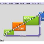
    Nevertheless, this is a big day for DDR4, as for the first time, Intel has announced DDR4 support in their desktop CPU roadmap. As for many protocols (USB 3.0, PCI express or SATA), Intel’s decision to integrate it within their processor or chipset is ringing the bell for this protocol wide adoption. If we take a look at the market segment where DDR4 is expected to be adopted first, the PC segment will surprisingly not come first, as it was the case for DDR3, DDR2 and so on. DDR4 adoption will first come from Enterprise, Servers and Storage SoC. The reason is crystal clear: the PC market is strongly cost driven, and the DDR3 memory chip cost is at its lowest today, when the DDR4 chip cost is still too high for the PC market. But the technical benefits linked with this new DDR4 protocol, like power consumption (but not only), justifies using DDR4 for these high end segments like Enterprise, Networking, Server or Storage. Would you ask the question if DDR4 could be used for high end laptop or media tablets (maybe less cost sensitive than desktop PC), the answer is no, as these applications will use LPDDR4 instead…

    If you take a look at the above picture, you can see that the DRAM Market revenues for PC is still higher than for Mobile handset in 2014… but not for long, as the market dynamics are clearly in favor of the DRAM segment for Mobile handsets and Media/PC Tablets, and this is not a real surprise. We may expect that DDR4 will be used in the enterprise market for the next two years, then in the Desktop PC segment when the DDR4 memory device price will have come down to the same level, or below DDR3 devices.

    If we take a look at the DDR performance scaling across time, we see that the internal performance (max. column cycle) has stayed almost flat. Thus, the DDR performance improvement (max. data rate) came from the “prefetch” mechanism, passing from 1 for SRAM to 8 words prefetch for DDR3. As a prefetch of 16 was undesirable, adding too much die area to the DDR4 device, the performance increase has been obtained by multiplexing two bank groups, keeping the 8 words prefetch scheme.

    Another DDR4 feature allows improving the noise impact due to Simultaneously Switching Output (SSO): Data Bus Inversion or DBI. Everybody who has ever been part of an ASIC design team knows that you must limit the number of output switching at the same time, or SSO, to guarantee a good enough noise margin. On the picture below, you can measure the SSO impact on the data eye, ranging from 410ps (no SSO) down to 350ps (32-b SSO). The data eye is directly linked with the available timing margin a designer will benefit to implement the SoC design. The shorter the data eye, the most difficult a design will be to manage!

    Another benefit linked with DBI is that you can get up to 30% power savings when using the feature. If you remember that one of the target applications is server farm, this 30% power savings can be extremely welcomed in this case, and good to have in any case.

    Another benefit of DDR4, especially important for enterprise systems is improved Reliability, Availability and Serviceability (RAS), thanks to the implementation of several features in the DDR4 protocol, like ECC, training and calibration, temperature monitoring, DBI, C/A parity check (with system retry), CRC, DDR4 Controller and PHY diagnostic register, to name a few.

    We have to remember that it took almost 10 years to JEDEC to come to DDR4 protocol release, one of the reasons being that the “4” in DDRn will certainly be the latest of this kind, the next SDRAM protocol being expected to be completely different (hopefully High Speed Serial SerDes based, with clock recovery to simplify both the SoC and the board level implementation). Thus, it appears that JEDEC committee has decided to implement has many as possible of the available techniques used to improve noise margin, power consumption and RAS. No doubt that the enterprise market will appreciate…

    From Eric Esteve from IPNEST

    More Articles by Eric Esteve…..

    lang: en_US


    Bluetooth Smart radio IP, backed by ARM

    Bluetooth Smart radio IP, backed by ARM
    by Don Dingee on 03-29-2014 at 7:30 pm

    For most devices, the on ramp to the Internet of Things means wireless, connecting a microcontroller or SoC via some kind of radio. It seems every merchant semiconductor company and embedded software firm has jumped on board the IoT wagon. There is a litany of chips, modules, operating systems, and protocol stacks already, and the list is growing daily.

    That is, if you want to buy something, or borrow an open source module or code. What if you want to design and build a low power chip for something like a wearable device, customizing it to your exact needs? After all, this is a fabless world today, and we don’t settle for just what parts are out there. ARM transformed the world once with processing IP, and is now positioning its resources to help connect the IoT devices its processor cores are being designed into.

    As we’ve discussed several times, on chip RF is no longer black magic, but there is still a certain amount of competence needed to make it work. With a depth of experience in radio technology among several founders earned while at Motorola, Sunrise Micro Devices emerged from stealth mode this week. ARM has backed Sunrise Micro with a capital investment and a couple key personnel on loan who know a thing or two about IP development, interfacing, and licensing.

    The first Sunrise Micro product in the CORDIO family is a Bluetooth Smart radio IP block, delivered as a hard macro in GDS II with link layer firmware support. The block is designed to an AMBA 3 AHB-Lite interconnect, with host-controller interface RTL to ease synthesis and simulation. There is also support for the radio within an ARM mbed prototyping board, and a separately licensable Bluetooth Low Energy protocol software stack.

    Sunrise Micro isn’t just using the words low energy; they’ve taken serious aim at battery powered and energy harvesting devices, designing the first 950mV radio with integrated power management including a capacitive DC-DC down converter for 1V or 3V operation. With remarkably low 6 mW transmit and receive power, optimized sleep and wake-up modes for the host processor, and riding batteries all the way to 1V, Sunrise Micro claims CORDIO BT4 can deliver an estimated 60% improvement in battery life compared to 1.2V implementations common today.

    CORDIO BT4 is also designed for simplicity, requiring only nine external components including the antenna for operation. The hard macro is currently optimized for the TSMC 55nm process, a mature CMOS node popular with microcontroller vendors today.

    Why wouldn’t ARM just acquire this company? A couple of reasons, the first being openness: ARC, Intel, MIPS, Tensilica, and others have embraced AMBA as their peripheral interconnect for IoT-class cores, opening the door for radio IP that could theoretically run with pretty much any architecture out there. Second is the Bluetooth radio and wearables focus, which many current ARM microcontroller customers are after – competing with them directly would not be good.

    The bet on Bluetooth Smart is extremely safe; with every smartphone to connect with, Bluetooth opens an immediate door to billions of users and devices. However, it is easy to see that Sunrise Micro CORDIO likely becomes a complete family shortly, targeting other IoT protocols with an equally ultra-low-voltage radio IP solution.

    For wearables and the IoT, in need of reliable and efficient radio IP, Sunrise Micro could be the answer.

    lang: en_US


    Care and trimming of MEMS sensors

    Care and trimming of MEMS sensors
    by Don Dingee on 03-28-2014 at 2:00 pm

    My first job in electronic design circa 1981 was making analog autopilots and control devices for RPVs – the early form of what today we call UAVs. A couple of really delicate boxes with gyroscopes, accelerometers, and magnetometers, and several boards full of LM148 quad op-amps surrounded by a lot of resistors and capacitors made the 17ft wingspan composite bird head in the direction we wanted.

    One thing I learned quickly was close only counts for horseshoes, hand grenades, and high-gain transistors. The care and feeding of op-amps requires a fair amount of trimming, in those days with the relatively new Bourns trimming potentiometer. By using a nominal resistor value in series with a potentiometer, we could finely trim the output of a control loop at a critical point – and then glue the knob with Loctite so it would stay there. (I still have a tray full of “pot tweaker” sticks somewhere in my electronics box in the garage.)

    Ah, if we could only make things digital, then all this trimming nonsense seems archaic. Digital circuits don’t drift with temperature. They compensate for design variation in software. It’s a good theory, except for one thing: it doesn’t magically work that way. At some point, the world is analog, and there is a sensor or a reference voltage or an oscillator that varies from its nominal specification, requiring some form of calibration.

    Apple discovered this the hard way on the iPhone 5S, really screwing up the bias on their MEMS accelerometer and failing to correct for it, resulting in big errors in apps. One “fix” was a software calibration routine that figures out the correct bias; note the caveat that the “surface is closer to flat than the existing bias of the device”, otherwise things can get worse.

    courtesy VentureBeat

    You may remember Apple has an M7 motion coprocessor (aka the NXP LPC18A1, an ARM Cortex-M3 microcontroller) between the MEMS sensor and the A7 processor itself, which probably saved them from the mother of all product recalls. iOS 7.03 fixes the problem, presumably (although Apple is pretty mum) updating the motion coprocessor firmware to grab a stored calibration factor and report a computationally-adjusted sensor reading.

    Without affixing blame between Apple and their MEMS sensor supplier, this is a hack that should have never escaped into the wild. Even a modicum of analog experience would have suggested factory calibration of the MEMS sensor, storing a value in non-volatile memory.

    Many MEMS sensors are being paired with a microcontroller, especially where the sensor is on a network readable by any number of nodes. This points to a best practice of local sensor calibration using one-time programmable memory such as the OTP IP offered by Sidense, a much lower cost approach than using the primary MCU flash to store fixed calibration values, and far smaller and more reliable than the ancient art of electromechanical trimming.


    The actual trimming operation varies, but usually takes two forms. Analog circuits can be altered directly by control of electronic switches from bits stored in OTP memory, typically adding or subtracting resistance to change a voltage or gain stage, or if an MCU is present on the sensor a computational factor can be permanently stored for firmware use. As MEMS processes become smaller, analog variation increases and trimming becomes more important.

    System-wide sensor calibration is an antiquated, time consuming, and expensive approach. As more MEMS sensors are showing up – automotive, fitness and medical, mobile, home automation – connected via networks, especially wireless sensor networks for the Internet of Things, the risk of an uncalibrated sensor reading propagating to multiple points gets bigger. With on-sensor trimming using OTP memory, every sensor delivers calibrated values every time, no matter what is reading them.