webinar IPXACT banner

Semiconductor IP Make the World Go Round!

Semiconductor IP Make the World Go Round!
by Daniel Nenni on 11-16-2014 at 3:00 pm

Semiconductor IP really does make the life of a semiconductor professional much easier which is why Google brings us so much IP traffic. If you look at the SemiWiki analytics, IP has always been a top draw. In comparison to standard EDA traffic, IP gets about 25% more views per blog on average. Synopsys is not only the leading EDA company they are also a leading IP company. Coincidence? I think not as semiconductor design and semiconductor IP go together like bread and butter. In fact, I would guess that more than 25% of Synopsys $2B+ revenue is IP related. For a quick history of Synopsys according to SemiWiki click HERE. A more complete history is in the EDA and IP chapters of “Fabless: The Transformation of the Semiconductor Industry.”


Synopsys started compiling their industry leading IP portfolio in 1993 through acquisitions and internal development. Here is a quick list of acquisitions, let me know if I have missed one (this does not include verification IP):

[LIST=1]

  • Compiled Designs (1993)
  • CADIS (1994)
  • Silicon Architects (1995)
  • Leda SA (2000)
  • C Level Design (2001)
  • InSilicon (2002)
  • Progressant (2004)
  • Cascade (2004)
  • Accelerant (2004)
  • TriCN (2004)
  • Virtio (2006)
  • MASAID (2007)
  • CHIPit (2008)
  • Synplicity (2008)
  • MIPs Analog (2009)
  • VaST 2010
  • Synofra 2010
  • CoWare Inc (2010)
  • Virage Logic (2010)
  • Inventure (2012)
  • Mosys (2012)
  • AMD IP (2014

    Synopsys has a nice DesignWare microsite here:

    Synopsys is a leading provider of high-quality, silicon-proven IP solutions for SoC designs. The broad DesignWare IP portfolio includes complete interface IP offerings consisting of controller, PHY and next-generation verification IP, analog IP, embedded memories, logic libraries, processor solutions and subsystems. To accelerate prototyping, software development and integration of IP into SoCs, Synopsys’ IP Accelerated initiative offers IP prototyping kits, IP software development kits and customized IP subsystems for rapid integration of IP into SoCs. Synopsys’ extensive investment in IP quality, comprehensive technical support and robust IP development methodology enables designers to reduce integration risk and accelerate time-to-market. Read more about why Synopsys is the Trusted IP Partner.

    Even more interesting, in my opinion, are the customer stories which you can browse by topic:

    Not only do you get to learn about IP, you also get to learn about the applications they are being used for and by whom:

    Fast Integration of DesignWare IP for PCI Express Enables Nitero’s First-Pass Silicon Success for Mobile 60GHz SoC
    “Selecting Synopsys DesignWare IP and design tools for our low-power NT4600 Wi-Fi SoC enabled us to integrate the IP in just a few weeks, helped us meet our aggressive tapeout schedule, and provided a seamless end-to-end design process, resulting in first-silicon success.” Sebastian Ahmed, Vice President of Engineering, Nitero

    Movidius Achieves First-Pass Silicon Success for Myriad 2 Vision Processing Unit with DesignWare USB 3.0, LPDDR3/2 & MIPI D-PHY IP “Selecting Synopsys DesignWare IP and design tools for our low-power, high-performance Myriad 2 VPU gave us peace of mind, a seamless and mature end-to-end design process, and most importantly, first-silicon success.” Sean Mitchell, Chief Operating Officer, Movidius

    Solarflare Achieves First-Pass Silicon Success for 10/40G Network Controllers with DesignWare IP for PCI Express 3.0
    “Using high-quality DesignWare IP for PCI Express for the last ten-plus years has helped assure our success in the competitive networking market.” Derek Roberts, Vice President of Hardware Architecture, Solarflare

    Bosch Achieves First-Pass Silicon Success for Consumer Sensor Application with Synopsys DesignWare NVM IP
    “We found the DesignWare NVM IP to be very easy to integrate and adopt. Selecting Synopsys IP is one of our risk-reduction techniques. DesignWare NVM IP allows us to minimize work on the memory interface and accelerate integration into the IC.” Horst Symanzik, Director of IC Engineering, Bosch Sensortec

    SunplusIT Achieves First-Pass Silicon Success for Webcam SoC with DesignWare USB 3.0 PHY & Controller IP “Our customers requested that we move quickly to upgrade our webcams to the USB 3.0 specification, so we needed reliable USB 3.0 IP. By using DesignWare USB 3.0 IP, our silicon rollout went exactly as planned.” G.T. Hsiao, R&D Manager, SunplusIT

    KYOCERA Designs High Performance Image Processing DSP for Next Generation Multi-Function Printer Using Synopsys Processor Designer “Synopsys’ reputation as an established provider of ASIP development tools, along with their multi-function printer design wins worldwide were key factors in our decision to use Processor Designer for the design of our optimized image processing DSP.” Michihiro Okada, General Manager of the Software 3 R&D Division, Corporate Software Development Division, KYOCERA Document Solutions Inc.


  • Complete SoC Debugging & Integration in a Single Cockpit

    Complete SoC Debugging & Integration in a Single Cockpit
    by Pawan Fangaria on 11-15-2014 at 10:00 am

    These days it’s common to expect large digital designs, analog blocks, custom IPs, glue logic, interfaces and interconnects all developed separately, perhaps by different vendors / teams, but integrated together in a single environment forming an SoC. The SoC can have multiple clock domains and can work in multiple modes of operations. Although different parts of the SoC may have been validated by respective teams, it becomes most difficult to understand all those components and verify all of them together at the time of integration in a single environment. Also, it’s gruelling keeping track of changes done by optimization, test and other tools. So, definitely, there arises the need for a versatile, intelligent tool and environment which can help easing pressure of debugging various parts of a design at different levels, interfaces and customizations in a single cockpit.

    While attending a webinarpresented by Gerhard Angst of Concept Engineering, it was clear that StarVision PRO provides the right kind of platform for analyzing and debugging today’s SoC designs. It has a complete digital interface for reading designs (either at RTL or at netlist level) in Verilog SystemVerilog, VHDL, LEF, DEF, and EDIF and so on along with various settings and options. The analog interface includes all Spice dialects, CDL, Spectre, Calibre, Eldo, SPEF, DSPF, and RSPF and so on. There is an expert cmd line interface which can read designs in different formats (such as Verilog, EDIF, Spice etc.) in succession, compile and merge RTL, netlist and Spice together and load the overall compiled design to view in the GUI.

    Multiple views along with simulation data annotated with the respective components and a separate waveform view can be seen at once in a single GUI. The waveform viewer can also be invoked separately to review large simulation data with particular, components, IOs or ports.

    In an SoC design, it may be possible that particular design blocks are not ready. A beauty of StarVision environment is that it supports top down design methodology by keeping the incomplete blocks and code for the same in ‘gray’ to be filled in later.

    A Clock Tree Analyzer can show a complete clock tree along with its interconnect logic. All clock domains can be viewed and their crossings can be analyzed at ease by using various available search options.

    The RTL can be visualized in free schematic, Process (for VHDL) or Always (for Verilog) styles while the RTL code remains the same. It might be possible that a VHDL Process code may be driving a Verilog Always code.

    Connectivity Lense is a great debugging feature which can expand connections to any port, and this can continue up to any level till the full path is traced. This feature works at all levels; RTL, Gate or Spice. At the Spice level, it can show all the transistors hidden with M-factor along with their connections. There is another path extraction feature which can extract and show a complete path between two ports or path(s) between a port and instance(s) of certain type. It can be used in various ways as desired.

    In a complex mixed-signal design, understanding and debugging Spice netlist is the most difficult task. StarVision provides multiple options such as netlist reduction (by merging transistors in series or parallel, parallel capacitors, serial resistors and so on), hiding the parasitics from the netlist, and automatic logic recognition to simplify a Spice netlist, thus making it easy for a designer to view and understand the Spice netlist.

    StarVision uses smart schematic generation algorithm; designers can switch between analog and digital schematic types to manoeuvre between different designs styles within an SoC.

    Post layout debugging, another difficult task, is supported by easy visualization and export of critical paths with netlists including resistances and capacitances. All formats including SPEF, RSPF and DSPF are supported. The extracted parasitic netlist can be viewed separately along with the transistor netlist. Any identified part of a circuit can be written out as Spice or Verilog for separate analysis and debugging, as is done for an IP.

    The StarVision environment also supports a number of UserWare APIs customized for designers’ productivity. Concept Engineering supports with the source code and documentation of these APIs for designers to develop their own new customized APIs or use the existing ones.

    The webinarcan be viewed for detailed information and also a nice demo on a design. Concept Engineering tools & technologies are also being exhibited at SemIsrael Expo 2014by their distribution partner KAL Katav Associates Silicon Technologies Ltd.

    Visit Booth #36 at –
    SemIsrael Expo 2014 Exhibition
    Avenue Convention Center at Airport City, ISRAEL
    November 25, 2014

    Contact info@concept.de and sales@edadirect.com for any more information.

    More Articles by PawanFangaria…..


    Are you SmarCoT or IoT?

    Are you SmarCoT or IoT?
    by Eric Esteve on 11-14-2014 at 4:00 pm

    No need to explain the IoT acronym (Internet of Things) except that IoT doesn’t really describe a reality: do you really know about any “Thing” being directly connected to the Internet? In fact, there is probably some intermediate system linking this thing with the Cloud, like a smartphone, an Internet box, a PC, etc. Just take a look at this picture below, more representative of the real life, showing the Aggregation Layers at the middle of IoT Edge Devices and Remote Processing.

    Thus, why not calling a spade a spade, and the “IoT Edge Device” a Smart Connected Thing, or SmarCoT…

    Smart because this thing really needs to be:

    • Smart=CPU: integrating a CPU, which brings intelligence to the thing, will be key, but not necessarily a CPU delivering several 100’s MIPS, rather a few.
    • Smart=Low Power: such a device needs to be power-aware, if not ultra-low-power. Do you really want to change or charge the battery every 5 days, or do we speak about several months if not years?
    • Smart=Low Cost: we think that SmarCoT will become popular and lead to the expected 10 Billion devices only if the final price is in the $5 to 10 range, leaving a maximum of $1 to 3 for the Silicon content. By the way, better to target 65/55nm node, or even 180/130nm than 28nm or 16FF, to reach this price tag.

    SmarCoT has to be connected because this is the concept foundation, which makes it attractive for the end user. It can be:

    • WiFi, but the protocol is quite power hungry…
    • ZigBee: the benefits are lower power (than WiFi or BlueTooth) and the mesh network capability, so you can build a complete personal area network, or use the mesh capability to reach more distant cell or base.
    • Smart Bluetooth (or BTLE): provides the same low power capability than ZigBee. Moreover Bluetooth technology is widely developed, and Smart BlueTooth is coming at the right time, also offering mesh capability. In fact, the market will decide which of these protocol will become dominant, all will probably be used (but not in the same system, because of cost and power).

    The last one, the “Thing”, can and will be absolutely anything, from a $300 watch targeting rich sportsmen to the $5 device still to be imagined.

    Another point: the business model related to SmarCoT is still to be created. Most probably the success will come for the creative enterprises building a complete system and the related software, generating monthly subscription or fees, rather than to the IC maker. Thanks to Handel Jones from IBS, this slide presented to Shanghai SOI last fall illustrates the functional model: the sensors in contact with the real (analog) world are connected through analog interfaces to a low power MCU and the eNVM, processing whatever is to process, the complete system being connected through BlueTooth in this example. The Power Management Unit will be mandatory to manage the battery in a low power fashion.

    What is the big piece on the above picture? Application software, and I would guess that this software will generate more revenue than the hardware!

    So, are you SmarCoT or IoT?

    This blog is not a poll… but feel free to give your opinion below.

    From Eric Esteve from IPNEST
    More Article From Eric Esteve


    SEMI Industry Strategy Symposium, Half Moon Bay

    SEMI Industry Strategy Symposium, Half Moon Bay
    by Paul McLellan on 11-14-2014 at 7:00 am

    Every January SEMI runs its Industry Strategy Symposium which is held at the Ritz Carlton in Half Moon Bay. This time it is January 11-14th. It is subtitled Riding the Wave of Silicon Magic.

    I find it a fascinating event to attend. There is a lot of information to be had in the presentations, of course, but also a lot from talking to attendees. The semiconductor equipment vendors are on the sharp end of fab buildouts and they know what equipment is being ordered and what is being pushed out. Equivalently, the materials people indirectly know a lot about running fabs, since if a fab isn’t consuming much material (such as wafer blanks) then it is not making much product. Attending the symposium thus gives a great overview of the manufacturing landscape and also a good insight into future process developments and some color on the slowing down (or stopping) of Moore’s law.

    As SEMI describes the conference:ISS 2015 explores the trends taking place in the industry from economic, market, technology, and manufacturing perspectives. In addition, the conference will look at ways to address the demands for continued development and manufacture of advanced technology. How should the supply chain respond to create increased value for customers, no matter where in the supply chain they reside? And most importantly, what should the industry do to maintain and increase prosperity to meet this demand in order to continue to sustain future growth? As always, the final goal is to help semiconductor industry executives set their strategies to navigate this exciting and rapidly changing environment.

    There are two keynotes. Scott McGregor, the CEO of Broadcom and Charles Toups, VP of Development Program Excellence at Boeing.


    The first day is divided up into two sessions. The first is Economic Trends with presentations from IHS, IDC, VLSI Research, Linx Consulting, and Stratfor. After lunch the session is Market Perspective with presentations from Samsung, Intel, Cisco, Gartner and CEA.

    The first session on Tuesday isTechnology & Manufacturing, with presentations from TSMC, Altera, Intel, Honeywell, Micron, imec and ASE. The second session is Opportunities at the Edge with presentations from Lux Research and Illumina (and another tbd).

    On Wednesday there is a presentation by McKinsey and then an executive panel session. It is moderated by Dan Hutcheson and the panelists are from Intel, JSR, TSMC and Qualcomm.

    That is a pretty impressive list of speakers and companies, and for sure that anyone who attends will learn a huge amount. And if you have never been there, the Ritz Carlton at Half Moon Bay is in an incredible location right on the beach.

    The full agenda for ISS is here. To register go here.


    More articles by Paul McLellan…


    Semiconductor IP Information Flow!

    Semiconductor IP Information Flow!
    by Daniel Nenni on 11-13-2014 at 9:00 pm

    One of the biggest challenges in the IP business, or any other business for that matter, is managing the information flow. Semiconductor IP is a critical piece of the fabless semiconductor ecosystem so anybody and everybody can write about it. Unfortunately, anybody and everybody ARE writing about it. From day one IP has been a big draw for SemiWiki and I don’t see that changing anytime soon, especially since IoT is a big IP play.

    One of the more clever IP communication channels I have seen this year is Cadence Whiteboard Wednesdays. These 3-5 minute YouTube video “chalk talks” are from experts in the IP world. Luigi Turnello for example, Luigi and I worked together at Virage logic helping the foundries with SRAM implementation. Look at his credentials, look at the patents, he is the consummate IP professional, someone who I listen to and learn from whenever possible, absolutely. Here is a complete list of what has been posted this year thus far. Hopefully they will continue:

    Whiteboard Wednesdays—Choosing the Right NAND Flash Solution In this week’s Whiteboard Wednesdays video, Lou Ternullo walks you through the steps to select the right NAND Flash solution and ensure it meets the requirements of your design.

    Whiteboard Wednesdays – The Evolution of NAND Flash In this week’s Whiteboard Wednesdays, Lou Ternullo explains NAND Flash and the need for advanced error correction. Lou also details the Berlekamp Chaudhuri Hocquenghem (BCH) algorithm. Learn how this algorithm is implemented and how engineers are using it in their designs today.

    Whiteboard Wednesdays—TripleCheck VIP In this week’s Whiteboard Wednesdays video, Moshik Ruben discusses TripleCheck verification IP (VIP) and how it allows engineers to know they have a thoroughly tested design that complies with the interface specification.

    Whiteboard Wednesdays—Verification IP Productivity Tools In this week’s Whiteboard Wednesdays video, Tom Hackett talks about Cadence Verification IP (VIP) productivity tools in the VIP catalog. These tools, PureView and TripleCheck, help engineers better match their VIP to their design under test ensuring better verified designs.

    Whiteboard Wednesdays—PCIe Controller Solution
    In this week’s Whiteboard Wednesdays video, Sandeep Brahmadathan breaks down Cadence’s high-performance, low-latency controller solution for PCI Express (PCIe).

    Whiteboard Wednesdays—Configurable 10/40G Ethernet Solution
    In this week’s Whiteboard Wednesdays video, Arthur Marris discusses configurable options for Cadence 10/40G Ethernet MAC, integrated PCS, and SerDes IP.

    Whiteboard Wednesdays—DDR Training Modes
    In this week’s Whiteboard Wednesdays video, Jeffrey Chung discusses the various training modes within the DDR interface. Watch to learn more about how these training modes can optimize timing.

    Whiteboard Wednesdays—Ethernet in Cars
    In this week’s Whiteboard Wednesdays, Arthur Marris introduces the next big thing in the Ethernet space—Ethernet in cars. With its high data rate, lightweight cabling, and distributed networking capabilities, as well as the fact that it is an interoperable open standard and works well with TCP/IP, Ethernet is ideal for addressing many of the challenges facing automotive engineers.

    Whiteboard Wednesdays—Selecting the Right PHY Solution
    In this week’s Whiteboard Wednesdays video, Kishore Kasamsetty reviews evaluation criteria when purchasing a PHY IP solution. Kishore details topics such as power, performance, and area (PPA), interoperability, DFI, and floorplan flexibilty.

    Whiteboard Wednesdays—Select the Right Performance for a 802.11ac/Advanced LTE AFE
    In this week’s Whiteboard Wednesdays video, Priyank Shukla removes the mystery behind choosing the right ADC in and Analog Front End for wireless (802.11ac and/or 3G/3G) communication systems.

    Whiteboard Wednesdays – Formal VIP for 100% Accurate Designs
    In this week’s Whiteboard Wednesdays video, Tom Hackett discusses formal verification IP (VIP), how it supports formal analysis, and how design engineers can leverage formal VIP to ensure their designs are 100% correct.

    Whiteboard Wednesdays—How to Verify SoCs Incorporating the M-PCIe Specification
    In this week’s Whiteboard Wednesdays video, Mukul Dawar provides an overview of the Mobile PCIe (M-PCIe™) specification. He explains how Cadence VIP for M-PCIe can help you verify your mobile SoC design.

    Whiteboard Wednesdays – USB Controller Connectivity
    In this week’s Whiteboard Wednesdays, Jacek Duda continues his discussion about USB controllers. This time, the conversation focuses on High-Speed Interchip Connectivity (HSIC) and Super Speed Interchip Connectivity (SSIC) and how they improve connectivity between multiple USB applications.

    Whiteboard Wednesdays – Verification Made Easy with Memory Models
    In this week’s Whiteboard Wednesdays, Tom Hackett explains memory models and their role in verifying memory interfaces in today’s SoCs. He’ll explain the differences between memory models and simulation VIP, and talk about how they can help make verification a little easier.

    Whiteboard Wednesdays – How to Support Higher Performance Multimedia Applications on Hosted Virtual Desktops
    In this week’s Whiteboard Wednesdays, Charles Qi continues his discussion on hosted virtual desktop applications, explaining how a growing number of users are increasing the demand for higher performance multimedia and user input processing.

    Whiteboard Wednesdays – Defining Different Types of USB Controllers
    In this week’s Whiteboard Wednesdays, Jacek Duda takes a closer look at different types of USB controllers and their roles in today’s devices.

    Whiteboard Wednesdays – Get to Know 802.11a/c Wireless Analog Front End Solution
    In this week’s Whiteboard Wednesdays, Priyank Shukla discusses Cadence’s wireless analog front end (AFE) solution for 802.11a/c.

    Whiteboard Wednesdays – See How Customizable Processors Can Help to Offload Your Apps Processor
    In this week’s Whiteboard Wednesdays, we take a little different approach and show you a fun and fast way to understand how Cadence® Tensilica® Xtensa® processors work, and how you can easily use them to offload your applications processor.

    Whiteboard Wednesdays – Verifying Solid State Drives Incorporating NVM Express
    In this week’s Whiteboard Wednesdays, Mukul Dawar explains the NVM Express protocol and considerations to keep in mind when using verification IP to perform functional verification.

    Whiteboard Wednesdays – Leading Up to PCI Express 4.0
    In this week’s Whiteboard Wednesdays, Moshik Rubin discusses the history of the PCI Express standard. Moshik starts with PCIe Gen1, which originated in 2002, and walks through the doubling of throughput offered by each new generation, ending with PCIe Gen4.

    Whiteboard Wednesdays – Using USB IP Controllers in Today’s Devices
    In this week’s Whiteboard Wednesdays, Jacek Duda follows up on his earlier video focused on USB performance and now takes a closer look at USB IP controllers and their roles in today’s devices.

    Whiteboard Wednesdays—Improving Power Optimization with PCI Express
    In this week’s Whiteboard Wednesdays video, Arif Khan takes a closer look at PCI Express and its role in improving power optimization.

    Whiteboard Wednesdays – Improving Hardware Verification with Accelerated Verification IP (VIP)
    In this week’s Whiteboard Wednesdays, Tom Hackett talks about Accelerated Verification IP (VIP) and how it makes hardware verification more efficient and productive.

    Whiteboard Wednesdays—Trends in the Mobile Memory World
    In this week’s Whiteboard Wednesdays, Kishore Kasamsetty discusses the low-power advantage that LPDDR4 provides over the LPDDR1/2/3 in the mobile market.

    Whiteboard Wednesdays – Taking Command of MIPI PHYs – M-PHY
    In this week’s Whiteboard Wednesdays, the second installment of a three-party series, Kevin Yee continues his earlier discussion on “taking command” of MIPI PHYs. Here, Kevin discusses M-PHY, its architecture, and the protocol’s functionality in mobile devices.

    Whiteboard Wednesdays – Promises and Challenges of DDR4 Memory Technology
    In this week’s Whiteboard Wednesdays, Kishore Kasamsetty provides a history on DDR4 technology. He also walks you through the improvements of DDR4 over DDR3, as well as the memory standard’s specifications and the challenges of meeting these specifications.

    Whiteboard Wednesdays – Verifying Your Designs with Simulation VIP In this week’s Whiteboard Wednesdays, Tom Hackett takes a closer look at simulation verification IP (VIP), and how these IP cores help verify designs with protocol checks, test sequences, and other capabilities.

    Whiteboard Wednesdays—Wireless Transceiver Implementations
    In this week’s Whiteboard Wednesdays installment, Priyank Shukla highlights wireless transceivers and protocol standards 802.11x and LTE/LTE-A. Wireless transceiver implementation options consisting of RF, Analog Front-End (AFE), and Digital components are examined.

    Whiteboard Wednesdays – Taking Command of MIPI PHYs
    In this week’s Whiteboard Wednesdays installment, Kevin Yee discusses what it means to “take command of MIPI PHYs”. This is a first of a three-part series on the topic. Here, Kevin will introduce you to D-PHY and its architecture, and how the protocol meets the requirements of mobile devices.

    Whiteboard Wednesdays – How IP Enhances Hosted Virtual Desktops
    In this week’s Whiteboard Wednesdays, Charles Qi introduces an emerging new application called Hosted Virtual Desktop, which supports increasingly mobile workers who want to use any smart, connected device to access corporate data resources. Charles goes into detail about how Cadence IP can help expand the application to help businesses make mobile workforces more efficient.

    Whiteboard Wednesdays – Comparing 3D Memory Solutions and Their Market Applications
    In this week’s Whiteboard Wednesdays, Scott Jacobson completes his three-part series on the Memory Wall with a discussion on the different 3D memory solutions today and their market applications. You may recall that in the first segment, Scott examined how CPU performance outstrips memory transfers, and discussed options available to system designers, such as 2D solutions.

    Whiteboard Wednesdays – Understand USB Controllers and Their Performance Specs
    In this week’s Whiteboard Wednesdays, Jacek Duda provides an informative overview of USB controllers and the potential performance that can be achieved. He also discusses in detail specs for USB 2.0 and USB 3.X. (Please visit the site to view this video)

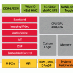
    Whiteboard Wednesdays—The Exploding Variety of New Interfaces for Mobile SoCs
    In this week’s Whiteboard Wednesdays, Tom Hackett focuses on the wide variety of new and updated mobile interfaces for mobile SoCs. These interfaces are broken down into three catagories—SoC fabric, memory, and chip-to-chip—and include ARM AMBA 4, ARM AMBA 5, OCP, DDR, LPDDR, LPDDR3, LPDDR4, Wide I/O, Wide I/O2, DRAM, eMMC, eMMC5, UFS, CSI-3, SoundWire, USB, PCIe, and SSIC. (Please visit the site to…

    Whiteboard Wednesdays – Why Cadence Verification IP (VIP) is a Smart Choice for SoCs
    In this week’s Whiteboard Wednesdays episode, Tom Hackett discusses why over 500 customers consider Cadence Verification IP to be the S.M.A.R.T. choice when looking to verify their SoC designs. (Please visit the site to view this video)

    Whiteboard Wednesdays – New MIPI Interfaces: Winners or Losers?
    In this week’s Whiteboard Wednesdays installment, Cadence’s Moshik Ruben takes a deeper look at the MIPI protocols that are the leading choice for certain mobile interfaces. Even though MIPI protocols are a top choice, however, they are being challenged by mobile versions of PCI Express and USB. Given this landscape, what does the future look like for MIPI and its challengers? Watch this short video to find out…

    Whiteboard Wednesdays—How 2D Solutions Help Close the Memory Wall Gap
    In this week’s Whiteboard Wednesdays episode, Scott Jacobson deep dives into 2D memory solutions like EMMC 5.0, UFS, and DDR4. Scott highlights how these solutions can help address CPU performance and power requirements and memory ability to deliver to these needs. (Please visit the site to view this video)

    Whiteboard Wednesdays – How the MIPI Alliance Works to Enhance Mobile Devices
    In this week’s Whiteboard Wednesdays episode, Moshik Ruben, Product Marketing Director at Cadence, highlights the MIPI Alliance’s focus on standardization to help improve today’s mobile devices. Moshik discusses MIPI protocols including CSI-2, DSI, D-PHY, SLIMBUS, M-PHY, UniPro, UFS, CSI-3, LLI and DDRF. This year alone, these protocols are projected to be shipped in over 4 billion mobile devices.

    Whiteboard Wednesdays – Implementing Always-On Audio
    In this week’s Whiteboard Wednesdays episode, Gerard Andrews, from the Tensilica Audio DSP Group at Cadence, discusses always-on audio functionality. Gerard details features like voice trigger, sensor fusion, and low-power audio playback, and explains how Cadence’s HiFi DSP solution can help you successfully implement always-on audio technology in today’s mobile devices. (Please visit the site to…

    Whiteboard Wednesdays – What is VIP?
    Today, our continuing Whiteboard Wednesdays video blog series will provide an overview of Verification IP and how it helps test today’s complex SoCs. Watch this week’s episode to hear Tom Hackett, product marketing director at Cadence, talk about the important role that VIP plays in the verification process. Tom details how VIP provides known good designs and stress testing for all interfaces and memory…

    Whiteboard Wednesdays—Imaging, Video, and Embedded Vision
    Today, our continuing Whiteboard Wednesdays video blog series will shed some light and provide practical insights on imaging video. In this week’s Whiteboard Wednesdays episode, Gary Brown, from the Tensilica Imaging and Video Division at Cadence, talks about imaging, video, and embedded vision technologies that are being worked on today. Gary gives a high-level overview of the industry sectors and end products…

    Whiteboard Wednesdays – Closing the Memory Wall Gap We’re excited to introduce Whiteboard Wednesdays, a new video blog series that will shed some light and provide some practical insights on how to address a variety of intellectual property (IP-) related design challenges. Our inaugural segment addresses the memory wall gap–that phenomenon that occurs when the bandwidth of microprocessors outpaces the bandwidth of the memory in the design, degrading system performance…

    More Articles by Daniel Nenni…..


    NoC 101, a Sonics Webinar

    NoC 101, a Sonics Webinar
    by Paul McLellan on 11-13-2014 at 7:00 am

    One of the things that I’ve been telling the people at Sonics when they will listen is that they should do a bit more basic education on Networks on Chip (NoC). Sure, the people who actually use Sonics’s products care about deep details such as security and power management, but there is a whole host of designers who have never used a NoC and have only the vaguest idea of what it is. Increasingly, designing an SoC is assembling a lot of IP blocks, perhaps hundreds, and a NoC is the best way to hook them up. It is prohibitively expensive in terms of area, power and design effort to put buses all over the chip as would have been done ten years ago. On November 20th at 10am (Pacific) Sonics are presenting an introductory webinar entitled NoC 101. I will be there to introduce the speakers and moderate the Q&A. The main speaker will be Drew Wingard the Sonics CTO.


    One of the things that a NoC does is separate functionality in way that makes the design much more flexible. If every block has to know about the bus architecture details then designers are forced to work at too low a level and the design becomes very tightly-coupled, as in the picture above. This is especially important when doing derivative designs, or taking a design from one generation to the next. Changing the communication architecture becomes an enormous task. In a modern process, wire delay can become dominant and can become the limiting factor of the overall system frequency.


    What a NoC brings is that it decouples the communication infrastructure from the blocks. The NoC can interface to any type of block, synchronous or asynchronous, new or legacy, different bus widths and so on. It means that designing and assembling the blocks is orthogonal to designing and implementing the communication architecture. If the performance is not met it is fairly easy to change the NoC. When a design goes from one generation to the next then the NoC goes too, and all the additional blocks for the next generation design can be added in a straightforward manner.

    The webinar will cover:

    • what is a NoC and why should I care?
    • design abstraction levels
    • limitations of the tightly coupled approach
    • using a decoupled NoC approach
    • design example using both approaches
    • clock and power domain crossing issues
    • NoC design input and verification
    • wrap up

    There will be a Q&A at the end of the webinar.

    Register for the webinar here.


    How many 28nm FDSOI SoC Design Starts in 2015? In 2020?

    How many 28nm FDSOI SoC Design Starts in 2015? In 2020?
    by Eric Esteve on 11-13-2014 at 4:28 am

    I would like to further discuss this graphic (presented during IP-SoC 2014 by John Koeter, VP of Marketing IP and prototyping, Synopsys) and focus on Active Design and Tapeouts at 28nm. In fact the very first activity appeared in Q1 2007, but it was only during 2010 that 28nm become popular, after the first Tapeouts coming in Q1 and an average number of active designs per quarter being around 75, to climb to 100 ranges during 2011 and 2012. To really understand this graphic we need to remember that the active design and Tapeouts numbers stop being reported in the graphic, but still exists in the real life! These numbers may still grow, and considering the 28/32nm shape, I would guess so. As you know, before going into production, an IC passes through active design (18 to 24 months), then Tapeout/prototyping/validation (another 6 to 12 months) before production ramp-up and full production. In other words, the active designs listed in Q4 2012 are most probably not yet into production today!


    The next graphic (presented by Handel Jones from IBS at the Shanghai SOI forum last September) represent the volume production wafer for the same 28nm technology node. This node is in full production for a couple of years, but you can see that IBS forecast that a higher wafer count will be in production in 2024 than next year in 2015! That means that 28nm will be the mainstream node for years, and we know the reasons: NRE cost far too high for 20nm and lower, and $/transistor cost inversion starting at 14/16nm. At least for a SoC design, integrating multiple CPU, memory and many IP, this 28nm node will be the best development cost/area/power compromise. If we consider the licensing agreement signed by Samsung for FD-SOI technology with ST-Microelectronics, starting at 28nm, we can expect higher design start count in 2015 than before on 28nm FD-SOI, as well as on the various 28nm flavors.


    You may be convinced that 28nm will stay the mainstream node for years, but wondering why 28nm FD-SOI should be used to support mainstream applications? In fact, we should look at FD-SOI unique value proposition, and extract the key arguments:

    • Wafer cost: SOI wafer processing need less mask levels (ion implants), compensating the current raw wafer overcost. When this overcost will decrease, due to higher SOI wafer consumption, the wafer final cost may be lower than for 28nm bulk.
    • Performance (Processor and digital logic) can be 30% better than bulk, thanks for the forward bias capability.
    • SRAM/TCAM deliver better performance and less power than nulk.
    • Analog & High Speed (SerDes for example) deliver better performance than bulk, and even more important, less variability.
    • Ultra Low voltage capability, unique to Fd-SOI, allow designing far better power efficient devices to address mobile applications and Internet of Things IC.


    Does it means that FD-SOI will canibalize 28nm node? No and there will be various 28nm derivatives and possible shrink, but this FD-SOI option will become more and more attractive in the future, as soon as a real IP ecosystem will become available. Don’t forget that one of the semiconductor giant is already supporting the technology, attracting the first IP vendors (like Cadence supporting DDR4 memory controller IP on 28 FD-SOI) and we can guess that some IP design teams are working to fill the needs of Samsung or Samsung’s customers.

    How many 28nm FD-SOI design starts in 2020? When and if the technology reach the mainstream IC design enterprises (most of them being located in China at that time), we can expect to count many more design starts in 2020 than in 2015, simply because 28nm should still be the mainstream technology node for cost-efficient SoC, and FD-SOI will have demonstrated the performance and power advantages on Silicon, and even more important in power-aware systems. It’s likely that doing evanlegization in China will be necessary, the discussion I had with Mark Ma during IP-SoC 2014 in Grenoble show that curiosity for FD-SOI is here, it will be time to further explain (again and again) why FD-SOI is Faster, Cooler and Cheaper.

    From Eric Esteve from IPNEST

    More Article From Eric Esteve


    Can Android1 Lead the Way for Google in New Smartphone Market?

    Can Android1 Lead the Way for Google in New Smartphone Market?
    by Pawan Fangaria on 11-12-2014 at 7:00 pm

    I had been wanting to write about it since Google’sbig bang announcement of Android1 in India in Sep this year and their associated strategy to capture some of the large pockets of Smartphone market within a matured or declining cell phone market and maturing overall market of Smartphone. Since I wrote my last article hereon maturation of Smartphone market in Feb this year, I have been happily watching how the P/Q factor is playing a major role in remaining untapped market in countries like India and China. Since an Smartphone is something, if not larger than life, at least ‘equal to life’ 🙂 utility item, P/Q factor will take more time to come down letting high priced Apple Smartphones to continue with a larger segment (who can afford that price) than just niche segment.

    I was pretty much convinced with Google’s India strategy of bringing high quality Smartphone with Android1 in it in the range of ~$100 and tie-up with top OEM partners including Micromax(next to Samsungin Smartphone shipment share and topmost in handset shipment share in India), connectivity partners like Bharti Airteland also on-line distribution channels like Amazon, Flipkartand Snapdealwho can proliferate into tier II and III cities. In another 2-3 years, Google expects Indian internet users to increase to 500M, most of them accessing internet through Smartphones. It expects to proliferate into all untapped regions including South Asia to get the next billion Smartphone users. After initial OEM with Micromax, Karbonnand Spice, Acer, Asus, HTC, Intex, Lava, Lenovo, Panasonic and Xolo will also make Android1 Smartphones.

    However, when I looked at Paul’s article – Xiaomi Already #3 in Smartphones Behind Samsung and Apple, I needed to re-look between Android1 phone and Xiaomi. While this again is in line with maturation of Smartphone market and need for high quality Smartphones within the range of $100 – $300, it appears to be a serious contender to Google’s Android1 strategy. Here is some of my analysis and I see a close fight between them to tap that remaining Smartphone market.

    I was perplexed due to the fact that when >80% Smartphone shipment is with Android OS, then how is it possible for Xiaomi with MIUI OS to become #3. But then on investigation I came to know that the ~85% number of Android devices includes ~20% of forked Android devices which is part of AOSP (Android Open Source Project). The MIUI OS is built out of AOSP and is giving severe competition to Google itself. It’s similar to iOS6 and MIUI app store is remarkable in the sense that it is similar to Apple’s. How could Xiaomi do it with AOSP? It’s mystery. But the truth is it’s a tough competition with Google itself. Does that mean Google should shut the open source? No way, that will again be a self limiting factor, because from the open source the innovation comes which proliferates Android per se. But in this situation, in a way, it’s asking Google to compete with itself, interesting!

    Let’s see some of the credible points about Google Android (in ~65% Smartphones other than AOSP based) powered by Google Apps and Play Services that provide the best features and security aspects. With everything of Google including Google Maps, Google Now, Google Translate, Google Games, Gmail, Hangout, Play Music, Play Books, and YouTube and so on, it makes a perfect Google world for a user. And YouTube is to let users watch videos offline in India where people may opt for lower data plans or slow speed economical internet options. I like this aspect of Google integrating things together which one may see distant apart.

    During Android1 announcement, Sunder Pichai clearly said that Google is getting into hardware, will provide reference platform to their OEM partners to choose between various pre-qualified components (processors, graphics, storage, battery, cameras…), all will be tested by Google and Android software completely optimized with these; clearly a good move towards providing high-end standard Smartphone with good quality at low cost for emerging markets. Android1 Smartphones will get processors from MediaTekand Qualcomm.

    What more? Android1 phone will get all OS updates in the same way as Nexus; it will get the latest updates of Android L, nicknamed as Lollipop! With Lollipop, the phone will get improved battery life, enhanced security features and smarter notifications. Users will be able to view and respond to messages from lock screen, hide sensitive contents, set priority mode for fewer disruptions, set ranking of notifications based on their senders and type of communication, set automatic encryption of data and so on. The features include natural motion, realistic lighting and shadows, and familiar visual elements to enhance user’s navigation experience.

    So, I see a definite merit in Android1 Smartphones based on their eminence in usability, integration, performance, screen accommodating most applications and the important one, price point. It will be a tough fight with Xiaomi, and who knows another AOSP based Smartphone can raise head; Gionee could be another.

    Let’s see how this game plays out in the emerging market for Smartphones. It’s going to be no road for Apple there and hard climb for Samsung with their high prices. It I look at my Feb article “Is Smartphone Market Maturing?”, the other leader Google seems to be promising with its Android prominence. But it has to be aggressive in the execution of its strategies.

    The verdict will be of audiences / users, their opinion and perception counts at the end of the day. Comments, opinions, suggestions are welcome!

    More Articles by PawanFangaria…..


    IP-SoC 2014 Top Class Presentations…

    IP-SoC 2014 Top Class Presentations…
    by Eric Esteve on 11-12-2014 at 1:00 pm

    … were given to an ever shrinking audience. This is IP-SoC paradox: audience has enjoyed very good presentations made by Cadence, Synopsys or ST-Microelectronic, to name just a few. As far as I am concerned, I was happy to present the “Interface IP Winners and Losers (Protocols)” in the amphitheater during the first day, enjoying some interesting questions about MIPI or UFS. This graphic was presented, showing the strong MIPI IP business 47% CAGR (but MIPI IP is an emerging segment) and also the sustained growth of DDRn IP (DDRn IP market weighting almost $100 million, is already mature) with a 34% CAGR:


    Let’s come back to the morning keynotes, with a presentation from Mark Ma, from Jiatao, a Shanghai based company representing various (western) IP vendors in China. Most of the slides are coming from a survey dedicated to the Semiconductor market in China, and these slides are worth to be carefully watched, you can go to D&R website for the complete slideshow “The Fortune behind Great Wall”. Just take a look at this one:

    Between 2009 and 2013 the total number of China’s IC design enterprises has grown from 472 to 583. If in 2009, 42% had an employee count below 50 and 55% between 50 and 500, this last number has grown to 74% in 2013. The start-up share is decreasing, and this means that China’s IC design enterprises are successful, as they can grow in term of employee count. By the way, more than 540 mid-size IC design enterprise, most probably fabless is simply huge! How many of these can we count in the rest of the world?

    What does such number means for the IP business? Just that if an IP vendor doesn’t target China yet, he should do it as soon as possible! There should be many opportunities, as China’s IC design enterprises are only supplying in 2013 less than 10% of what’s consumed in China (this slide).

    Synopsys and Cadence’s presentation are always very interesting. Both companies could decide to present their IP port-folio (that you can see on their web site), but Cadence and Synopsys have been creative and have presented attractive presentation. Let’s start with Synopsys and john Koeter sharing the active design and tape out count by technology node, for every quarter during the last ten years:

    If anybody still has a doubt about Moore’s law landing around 20nm node, just take a deep look at this slide. You will see that the active design count has been in the 150-200 range per quarter for each node from 90nm to 28nm and that the cumulated active is higher for 40/45nm than 65nm. In fact, it took probably longer to design at 40/45nm than at 65nm, which stayed two years less on the curve than 40/45nm. Also very interesting is the number of Tapeouts for 16/14nm (in the 40 range) in Q3 2014, much higher than the Tapeouts count for 20/22nm in Q1 2013, at the highest level with 15 to 20. Clearly, the 20/22nm node will be skipped as the Tapeouts count in Q3 2014 is… zero!

    The above slide from Synopsys about Power Harvesting Method is an illustration of the creativity that I have above mentioned. I let you dig into the slide…


    Amir Bar-Niv from Cadence has spent some time to explain the specificities of Analog, starting from the high level economics (above) to go down to analog design challenges in FinFet. The next slide is also interesting as it shows that Cadence is really committed to the IP business: this list of “1[SUP]st[/SUP]” includes from 28nm Low Power PCIe 3.0 SerDes to FinFet 16G SerDes… passing by Silicon proven DDR4 in 28nm FD-SOI. A clear illustration of what will be needed to build an IP ecosystem to support 28nm and 14nm FD-SOI technologies, but DDR4 is just a starting point…

    From Eric Esteve from IPNEST


    Xilinx Creates Worlds Fastest, Densest, DSP Rich FPGA and Shipping Now

    Xilinx Creates Worlds Fastest, Densest, DSP Rich FPGA and Shipping Now
    by Luke Miller on 11-12-2014 at 10:00 am

    Xilinx, last week announced that it has shipped the 20nm Kintex-115 Device, and I quote:

    “Xilinx has produced a 20nm FPGA for data center acceleration called Kintex UltraScaleKU115 FPGA.
    The chips deliver up to:

    · 1.16M logic cells,
    · 5,520 optimized DSP slices,
    · 76 Mbits of block RAM,
    · 16.3Gbps backplane-capable transceivers,
    · PCIe Gen3 hard blocks,
    · integrated 100Gb/s Ethernet MAC and
    · 150 Gb/s Interlaken IP Cores, and
    · DDR4 memory interfaces operating at 2,400 Mb/s
    · 2 Flux Capacitor Cores (1.21 Jiga Watts per core for time travel)”. Just checking if you’re still reading.

    Two area’s I would like to draw your attention to is:

    1) The number of DSP(5520), speed(741 MHz), and bits (27×18)
    2) GT’s : Gigabit Transceivers, speed(16.3 Gbps) and density (64)

    I think I need to remind us that only about 12 years ago, the Virtex-II Pro50 had 232 DSP. We are so spoiled today, 5220 DSP? Yikes. Just think about the amount of work this one FPGA can do. It is definitely not midrange and the FPGA blob strikes again as this one Xilinx FPGA just ate a whole rack of 6U cards from 10 years ago.

    Just as important as DSP is moving data on and off the FPGA via what I will call the ‘Serial Revolution’. Serial interfaces do make sense right? Over the years we have been able to witness, TTL/CMOS –> LVDS/DDR–>GTs. Less IO, more bandwidth and lower power. Ok, yes there is higher latency going serial which can be overcome with faster FPGA clocks and some architecture changes. The Serial Revolution is not only striking the Xilinx FPGAs but it is allowing data converter companies like TI, ADI to reduce the IO demands of high speed/high bandwidth data converters using JESD204b over GT’s. This means a data converter that needed 64+ LVDS IO, can be reduced to 5 lanes of JESD204b. For example if you had a digital receiver design 5 years ago, you were hard pressed to get 2 ADC’s to feed one FPGA over a Giga Sample. Not anymore, easily connect 8-12 of these puppies depending on the system requirements.

    Not only can you use JESD204b but also Hybrid Memory Cube (HMC) as well. By the way, Xilinx 28nm handles HMC and JESD204b also, that is why it is important to look at Xilinx not at a certain technology node but as a portfolio of solutions. You may not need 5520 DSP, nor 64 GTs. See how Xilinx fits into your design but it does not always have to be the newest fastest process, though it is tempting. The table below captures the trade offs of Xilinx 7 Series compared with Xilinx UltraScale. Also remember the 20nm UltraScale has a new DSP, which means when performing complex multiplies you only need half the DSP in 20nm when compared to the 28nm, 7 series. That is very important and very powerful especially of you design is using complex arithmetic.

    The Xilinx DSP in the 20nm family are the world’s fastest, widest, densest DSP. Raw fixed point arithmetic will give you about 8.2 TMACs, and about 1.3 TFLOPs. So do you think it is wise and efficient to program this puppy the old fashioned VHDL/Verilog way? You can, but for real productivity, Vivado HLS will really lighten your load enabling you to code the design in C/C++. This means real portable libraries, faster simulation times and less errors at system integration. A white paper that I wrote,wp452 highlights the power of HLS by tackling one of the hardest problems to solve in silicon, which is complex floating point matrix inversion. At 8.2 TMACS, 1.3 TFLOPs Xilinx once again has shown the world that they are the FPGA leader, and more than that, they are an EDA leader as well as a SoC Company. So I encourage you to familiarize yourself with the family of Xilinx FPGAs and see for yourself why Xilinx is the Global FPGA leader. Click Here