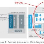
SerDes stands for Serializer/Deserializer, and SerDes is a serious piece of design, requiring an extremely experienced team of analog engineers (below 10 years’ experience, you’re still a quasi-beginner). Better to rely on an analog guru to draw the SerDes architecture and manage the team! Why does SerDes is becoming more and more important? At first, because next-generation peripherals, tablets, servers, and other applications are demanding greater bandwidth at lower cost and power. To meet these demands, communications protocols like PCI Express® (PCIe®) have gotten substantially faster—PCIe Gen4 calls for signal transmission speeds of 16Gbps. Such a protocol based function (PCIe, MIPI, SATA, etc.) is made of: Controller (100% digital) + PHY.
The PHY itself can be broken into a (PIPE interface + Physical Coding Sublayer (PCS)), both digital, and the famous SerDes. We could imagine running some of the SerDes functions by using Digital Signal Processing (DSP) circuitry, but the power consumption would explode, thus SerDes are completely analog, based on full custom design. The second reason why SerDes design is becoming more critical as bit rate goes up (16 Gbps for PCIe 4, 28 Gbps for certain communication protocols) is because it requires to add new design techniques to compensate the channel losses (as high as 27dB at Nyquist for PCIe 4) AND keep the power consumption as low as possible.
Until I read this white paper from Cadence, I was under the impression that I knew enough about SerDes design technology to be able to discuss about SerDes, during a conference or a show… but I learnt so many new design and architecture features that I really suggest you to read this white paper “Defining a New High-Speed, Multi-Protocol SerDes Architecture for Advanced Nodes” from Cadence.
Let’s try to summarize the main points.
The author claims that a SerDes supporting the latest communications protocol specifications, including PCIe, calls for a new type of SerDes archi*tecture that addresses the following needs with minimal power dissipation:
- Data and clock recovery requirements in high-speed, high-dB-loss, and high-crosstalk channels
- Critical loop timing specifications for the DFE
- Environmental and process variations
- Transmitter performance under low-supply conditions
- High-speed clock distribution
Each of these points will be made explicit during the course of a white paper. Please remind that the paper describes a SerDes supporting “Multi-Protocols, and multiple processes nodes, going up to 16nmFinFET.
Clock generation and distribution
For clock generation and distribution, a low-jitter clean-up phase-locked loop (PLL) in the common area allows the use of a cost-effective reference. Un-buffered clock distribution on high-level metal avoids jitter that’s induced by power supply noise. The architecture also includes an in-lane local PLL operating at the TX baud rate.
Dual-path Reception
Traditional SerDes architectures have a limit in maximum achievable equalization. Typically, the DFE can’t begin opening the eye until clock recovery has occurred. Clock recovery, in turn, can’t start until the eye is slightly open. Also at odds are clock recovery and data recovery continuous time linear equalizer (CTLE) frequency response. Thus the architecture consists of separate optimized paths for clock recovery and data recovery. For each path, the relative timing is adjusted by an adaptive loop, which saves power. Decoupled clock recovery also allows for much better jitter tolerance because the CTLE and edge samplers are optimized for the clock path. Unlike many SerDes architectures, this new architecture allows use of every edge in the data stream for clock recovery.
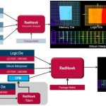
The optimized clock path gets more signal and less noise than in a single-path design, due to a number of factors. For one, a separate CTLE for clock recovery, shown in the lower portion of Figure 3 (above), allows high-frequency peaking optimization for clock recovery. The equalizer is converged at the clock sample time, without having to rely on incorrect discrete equalization converged at the data sample time. And, all data patterns can contribute to clock recovery.
In Figure 3, the red blocks show the adaptive loops in the receiver. A digital controller manages all of the loops. Some of the adaptive loops are for start-up only. Others run in the background, so if there are changes in, for instance, humidity or temperature, then the backplane automatically adjusts to accommodate the changes. This approach allows continuous uptime, as the background adaptive loops do not interrupt the flow of data through the system.
Hybrid Tx Path
The hybrid TX path (Figure 4) in the multi-protocol, high-speed SerDes architecture is designed with a hybrid driver with true emphasis, not just de-emphasis. This path offers better rise times due to boost circuit, lower output cap than H-bridge, and less wasted power in de-emphasis. The hybrid TX path addresses transmitter effects by:
- Maintaining power advantages inherent to non-emphasized voltage mode
- Allowing additional amplitude in excess of what the voltage mode can produce
- Requiring less power in emphasis than conventional voltage mode or current mode driver
- Allowing, through the use of broadband matching, the use of larger and better protecting electrostatic discharge (ESD) diodes
Since the data path is a full-speed DFE, it avoids the substantial increase in required circuitry and clock distribution that unrolling would need. In addition, the IP:
- Eliminates the need for a critical IQ phase-aligned clock distribution
- Uses a reduced area and power, wide-frequency-range phase interpolator
- Features lower frequency, top-level clock distribution
Summary
A new multi-protocol, high-speed SerDes architecture, designed for advanced nodes, addresses all of the existing and new challenges while offering the following characteristics:
- Support for data rates of 1Gbps up to 16Gbps, with a continuous frequency range
- Compliance with:
- PCIe Gen4: 2.5Gbps, 5Gbps, 8Gbps, 16Gbps
- 10G-KR: 10.3125Gbps, 12.5Gbps
- XAUI: 3.125Gbps
- RXAUI: 6.25Gbps
- Gigabit Ethernet/SGMII: 1.25Gbps
- SATA: 1.5, 3, 6Gbps
- HMC-SR: 10Gbps, 12.5Gbps, 15Gbps
- Equalization up to 30dB channel loss (in the presence of -48dB crosstalk)
- Low power
- Flexibility and robustness
An IP vendor targeting the interface IP market, expected to grow with 10%+ CAGR until 2020, has to propose an integrated solution (Controller + PHY) on the market. This means that such an IP vendor has to perfectly manage SerDes design technology, not only on the mainstream, but on the advanced nodes like FinFET 16nm, supporting data rate up to 16 Gbps. Developing such a multi-protocol SerDes is a real challenge, but the ROI will be high. In fact, the market demand for higher bandwidth is growing incredibly fast: every year, the demand for storage is growing by 60%. Before storing data you need to exchange it and increasing system bandwidth is a good way to keep the size and cost of networking system reasonable. But you need to increase the various protocols (Ethernet, PCI Express, etc.) frequency, and to do so, you need new, power efficient SerDes.
Learn more about Cadence’s multi-protocol, high-speed SerDes PHY IP at:
http://ip.cadence.com/ipportfolio/ ip-portfolio-overview/interface-ip/serdes-ip
By Eric Esteve from IPNEST