webinar IPXACT banner

How many coats cover this SoC?

How many coats cover this SoC?
by Don Dingee on 03-11-2015 at 7:00 pm

“Most interior paint covers with one coat.” Back when there was something called a newspaper, this was an actual blurb in the home improvement pages, section 3, part 8, page 5 of the Chicago Tribune on Sunday, August 13, 1961. Even then, marketers were catering to consumers looking to cut corners and save time, and one-coat coverage was a popular claim among pigment providers. The column filler went on to say yellow and pink have low covering power, and may need a primer. Let’s face it, pretty much nothing covers dark green in a single application.

I suspect most SoC verification teams don’t trust that claim any more than they trust code coverage tools. To counter the lack of confidence, teams usually keep applying coats of testing until they see a functional coverage metric asymptotically approaching 100%. There is no arguing with 100%, right? Nobody gets away with walking into a meeting and saying we’re good, coverage is at 85%. The effort to get to 100% is usually accepted – expected, in fact.

Cutting corners on painting can be somewhat hazardous. One risks the scornful review of a significant other, who visually inspects the work on two dimensions: “you missed a spot”, and how much of a mess was made in the process. Too little paint is bad; leftover paint is a bonus for future maintenance. The actual amount of paint used, and the number of brushes or rollers chewed up, is rarely a consideration if the budget was met and the aesthetic outcome is right.

Cutting corners on verification can be deadly. However, verification differs from house painting in one important way: different tests deliver varying amounts of effectiveness and coverage. A difficult-to-cover dark green spot in an SoC design may require a focused verification routine. Wider swaths of HDL may be covered more easily and quickly.

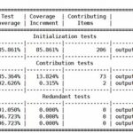
The question for SoC verification becomes how to provide the greatest code coverage in the least amount of time and effort. Some tests may prove better than others, and some tests may prove to be completely redundant adding no value. Most verification tools only report on the final result – coverage. Teams may be trying to fill in coverage and expending significant resources on duplicative or ineffective tests, and never know it.

Aldec has released Riviera-PRO 2015.02 with a major new feature: test ranking. By looking at how tests contribute to coverage, comparisons become easy to spot. Teams can put more energy into higher ranked tests, and less into tests that are redundant or produce poor contributions.

There is also a cost factor to the ranking. Parameters can include how much simulation time is required; where two tests provide equivalent coverage, the faster one should be chosen. A longer test may be worth the CPU cycles if it provides substantially better coverage than alternatives.

Test ranking provides a unique and valuable view of the verification process. Aldec continues to expand Riviera-PRO, combining simulation, debug, and reporting into a single productivity tool for advanced verification.

Related articles:


SoCs More Vulnerable to ESD at Lower Nodes

SoCs More Vulnerable to ESD at Lower Nodes
by Pawan Fangaria on 03-11-2015 at 1:00 pm

Electro Static Discharge (ESD) has been a major cause of failures in electronic devices. As the electronic devices have moved towards high density SoCs accommodating ever increasing number of gates at lower process nodes, their vulnerability to ESD effects has only increased. Among the reasons for ESD failures in SoCs, device breakdown and interconnect melt-down account for more than 70% of the overall ESD failures. Long term reliability is anyway at stake due to such ESD issues; they can even impact the first silicon success.

Look at how the ESD design window for MOS devices has shrunk as the technology node moved from 130nm to 32nm. The margin between operating voltage and oxide breakdown voltage has continued to decrease, making a device more prone to breakdown due to ESD. High current flow through unintended paths due to any kind of ESD effect (Human Body, Machine or Charged Device Model) can render the device to failure. To protect the devices from ESD, it’s important and essential to introduce effective clamp circuits with I/O and P/G pads that can handle large transient currents, provide efficient discharge paths to ESD currents and prevent any pin voltage from exceeding the oxide breakdown voltage.

In aDAC 2014 presentation I found that PathFinder from ANSYS is a state-of-the-art tool that can precisely check the resistances of signal bus, power bus and the power-to-ground path to help designers appropriately plan protection circuits for device breakdown due to any ESD event.

If we look at the interconnect scenario, that also has become extremely vulnerable at lower technology nodes with ESD current limits going down significantly. Any current crowding on ESD devices or insufficient wire width on ESD pathways can cause melting of associated interconnect. Appropriate signal and power buses and clamps needs to be planned to prevent interconnect melt-down.

ANSYS PathFinder can precisely define CD limits for interconnect and check it for signal bus, power/ground bus, and the power-to-ground path, thus helping designers appropriately plan for the buses and power-to-ground paths and prevent their melt-down due to any ESD event.

Today, an SoC can have multiple IPs and blocks under different power domains. This also can give rise to cross-domain ESD issues if not properly analyzed and taken care of.

Above is an example where ESD discharge can pass through an unintentional path causing failure. The circuit must be analyzed for such eventualities and protected from ESD.

PathFinder performs cross-domain CD checks, bus resistance checks, and clamp connectivity checks to prevent such ESD issues that can arise at the boundaries of different domains.

Thus PathFinder provides a powerful solution for accurate ESD analysis and prevention of ESD issues in both, IP and SoCs. It takes layout, technology information, Spice netlist including clamp models, and ESD rules as inputs and then performs all kinds of checks including resistance check, interconnect failure check, layout connectivity check, and dynamic CDM checks for IPs. The PathFinder can be used from very early stages of a design such as I/O pad planning, I/O ring planning, and floorplanning until the final sign-off. It has very easy-to-use GUI for debugging and finding root causes of issues, and fixing those. The tool is robust enough with capacity to handle full-chip analysis including its package.

This ESD solution using PathFinder is part of ESDA(ESD Association) reference flow and TSMC reference flow.


Innovus: Cadence’s Next Generation Implementation System

Innovus: Cadence’s Next Generation Implementation System
by Paul McLellan on 03-11-2015 at 7:00 am

Yesterday was the first day of CDNLive. There were three keynotes. The first was by Lip-Bu Tan, Cadence’s CEO (and the Chairman of Walden International that he will be the first to remind you). The most interesting tidbit was that Cadence now has over 1000 people working on IP and that it represents 11% of their revenue. Then he announced Innovus, Cadence’s next generation of physical design (much more below).

The second keynote was by Simon Segars, the CEO of ARM. He painted a vision of how the mobile phone will eventually become the only device you need, holding your plane tickets, passport, car keys, house keys, thermostat control and so on.

He also outlined how the datacenter environment is changing from simply being mobile device and huge cloud datacenter, to having intelligence distributed through the network too. Of course, Intel does not necessarily have the ideal products for this and it is a big opportunity for 64-bit ARM. Although ARM does not have the single process performance of a high end Intel processor, it has much lower power, lower cost, easy to integrate and so smaller physical size, and very high throughput due to the large number of cores possible.

But the most interesting keynote was the third, by Anirudh Devgan, SVP of Digital and Signoff. I think that means that if it ends in “-us” then he has it in his organization. And he has one more product in his portfolio after today, Innovus. This is Cadence’s next generation physical design, rebuilt from the ground up and tied in tightly with all the already-announced analysis tools such as Tempus and Voltus. The key big picture numbers are that it is 10-20% better PPA than Encounter and 5-10X faster.

Anirudh jokingly said that when he joined Cadence, if he went to a bar people would say “Cadence is pretty good, but they need to improve their placement.” Well, Innovus has a completely new placement engine, GigaPlace and a new optimization engine, GigaOpt. There is a new advanced clcok design system based on the Azurro acquisition from a couple of years ago.

Innovus has been with initial customers for quite some time, so that now that the public announcement is here it already has success stories and a track record of results.


On run-time above are several designs. The top one is 9.3M cells in 28nm where the speedup is almost ten times, from 700 hours to 70 hours in round numbers. The last design is a mobile SoC which went from 150 hours to 29 hours (not quite scraping under the day) for a 5X speedup.


But running fast is nice, but ultimately results are what count. Power, performance, area or PPA. The above graph shows a microprocessor design (no idea whose but the previous methodology was manual which has to narrow the field quite a bit, but being 16nm not 14nm means it is not the company I first thought of). The old manual design took a long time and gradually crept closer to the goal (the hard to see blue line). With Innovus, not only was the goal reached much faster, but it was exceeded (the red line).

There are rumors around that Cadence has won Apple away from Synopsys. Of course nobody can comment on this. When I heard the rumor it made little sense since Cadence is also rumored to have lost pretty much every benchmark below 28nm with Encounter so it seemed unlikely Apple would be an anomaly. But if it is Innovus then the rumor is much more credible.

ARM have been using it with the Cortex-A72 (their new core announced a month ago). As Noel Hurley, who is general manager of the CPU group, said:At ARM, we push the limits of silicon and EDA tool technology to deliver products on tight schedules required for consumer markets. We partnered closely with Cadence to utilize the Innovus Implementation System during the development of our ARM Cortex-A72 processor. This demonstrated a 5X runtime improvement over previous projects and will deliver more than 2.6GHz performance within our area target.

Apologies for the poor quality of the images. I wasn’t given a copy of the presentations so these are all photos of the screen. But I figured getting the information out quickly is more important.

Details of Innovus are on the Cadence website already here.


On-Chip Power Integrity Analysis Moves to the Package

On-Chip Power Integrity Analysis Moves to the Package
by Tom Simon on 03-11-2015 at 1:00 am

Power regimes for contemporary SOC’s now include a large number of voltage domains. Rail voltages are matched closely to the performance and power requirements of various portions of the design. Indeed, some of the supply voltages are so low that the noise margins in these domains is exceedingly low. Higher voltage domains are still imbued with tight power rail noise margins due to performance needs. In either case designers have good reason to be concerned with power integrity. If the dynamic operation of the chip causes power or ground excursions, chip operation could be imperiled.

EDA companies have been working on di/dt on-chip analysis solutions for a long time. When I was at Sequence around 2002, this was a hot and heavy area of product planning and development. Sequence was ultimately acquired by Apache, which has since become part of ANSYS. But the initiative that emerged back then is still going full force.

ANSYS has long has had a solid and commercially well accepted offering in this space – RedHawk. But as a recent white paper from ANSYS points out, looking at power integrity on the chip by itself, assuming ideal connections to the power pins, is not sufficient to ensure design success. The package plays a significant role in determining the power integrity of a design. The power grid is fed by numerous C4 bumps on the die. There is nothing ideal in power delivery through today’s flip chip packages.

ANSYS points out that the package nets need to be modeled individually, not lumped together or aggregated. The modeling should include full RLCK effects as well. The approach that ANSYS’s RedHawk-CPA, chip package analysis, uses is to extract the package using a 3D FEM extractor. A big benefit of this extraction based approach is that it yields highly accurate results in a SPICE netlist format, instead of an s-parameter that you would get from a full field solver. Field solvers are necessary in the RF and high frequency range, but for power integrity the extraction approach is fine, and offers real benefits.

S-parameter data have return path information embedded in them, so isolating power and ground issues is complicated. S-parameters are good in frequency domain analysis, but what is needed here is transient analysis, which RLCK models excel at. The RedHawk-CPA flow used in conjunction with RedHawk provides for dynamic or static analysis of power integrity in various modes of operation. The difference when package information is included is dramatic.

Reading in package data is made simple for the IC designer with the ability to import SIP, ODB++ and MCM formats. Bump net assignments are handled by reading in a PLOC file. Of course this can be modified manually as well. By working with actual bump impedance values and package level decaps, RedHawk-CPA affords more realistic voltage drop and dynamic power grid performance results than would be achieved with estimates or less rigorous analysis.

At the end of the process a chip level model for power grid analysis is created that the package designer can use to optimize the package.

There are some nice visualizations available after the analysis. I am including some below. The resulting data can be used to visualize voltage, current maps, or waveforms. It also supports near and far field EMI computations. This is where ANSYS’s multi physics expertise comes in.

SOC designs are operating with speed and power requirements that push them to the limit of present technology. The main side effect of this is that nothing can be designed without consideration of other elements of the whole system. To read more about RedHawk-CPA for including package information in your power integrity analysis download this white paper.


Altera 14nm and 10nm Update!

Altera 14nm and 10nm Update!
by Daniel Nenni on 03-10-2015 at 7:00 pm

In preparation for this blog I Googled around to get the latest information made available by Altera to see if it matches up with what I know from discussions amongst the fabless semiconductor ecosystem companies. Unfortunately when I Googled Altera+20nm+14nm the first three entries from the Altera website were Error 404 Page Not Found. Just a heads up, no big deal, sitemap errors happen to the best of us.

The real reason for this blog was to make it perfectly clear that I do not now nor have I ever believed that Altera would leave Intel for TSMC at 10nm. The Altera CEO made an unfortunate comment during the last conference call that Paul McLellan mentioned in his blog Altera Back to TSMC at 10nm? Xilinx Staying There. To me this was a leadership fail more than anything else. Publicly shaming your foundry partner is really a bad idea. It is like publicly shaming the chef before your meal has arrived.

Here are my top 10 reasons why Altera will NOT leave Intel at 10nm:

[LIST=1]

  • Millions of dollars have been invested for Intel design enablement
  • Intel has a density advantage at 14nm and again at 10nm
  • Moving from Intel 14nm to Intel 10nm should not be difficult
  • There is no way Intel Custom Foundry would allow it to happen
  • Intel CEO endorsed the Altera relationship at Goldman Sachs Conference
  • If the Intel relationship fails it could cost the Altera CEO his job
  • Altera is at a competitive disadvantage using the same foundry as Xilinx
  • Altera would be better off moving to Samsung Foundry than TSMC
  • Because I said so
  • Altera hired the Intel FinFET design implementation team from Tabula

    Tabula was the first Intel Custom Foundry customer, right? Seriously, would Altera have hired the Tabula design implementation team if they were switching back to TSMC? Great move by Altera hiring a team with serious FPGA FinFET experience by the way. Xilinx should have been all over the Tabula carcass the the day SemiWiki broke the story: TabulaCloses its Doors

    If you think I’m wrong please say so in the comments section but I’m not so you probably shouldn’t waste your time.

    The other thing mentioned on the conference call was that Altera has not taped out at 14nm yet. From what I hear it won’t happen until later in Q2 so do not expect to hear champagne bottles popping on this coming conference call (April). What is the problem you ask? Let me share with you my opinion, observation, and experience as we bloggers do:


    In any big fabless semiconductor company there are different design implementation teams. Let’s call them the A-Team and the B-Team. The A-Team does the first implementation and the B-Team does the follow-on design iterations. From what I understand the Altera A-Team, which is here in Silicon Valley, was still busy with 20nm so the Altera Penang (Malaysia) team was tasked with 14nm and the result was a delayed schedule. Now that Altera has the Tabula design implementation team here in Silicon Valley they will finish the 14nm tape-out then start Intel 10nm. Just my opinion of course.

    Also Read: 2015, the Year of the Sheep…And the 16nm FPGA


  • FinFET Design Enablement

    FinFET Design Enablement
    by Daniel Payne on 03-10-2015 at 1:00 pm

    We read about FinFET technology in the semiconductor press daily now, thanks to Intel introducing their TriGate transistors starting in 2011 and creating a race with foundries and IDMs to switch from planar CMOS nodes. To get some perspective about the progress of FinFET IP and EDA tools I spoke with two experts from Synopsys, Swami Venkat and Saleem Haider. Synopsys is an EDA software company that enables FinFET chips to be designed, verified and implemented. We spoke by phone on Friday, March 6th.For the past three years 2012-2014, the general FinFET progression has been mostly test chips and limited production, outside of Intel. At DAC in June 2014 we saw the first 14 nm FinFET production silicon from Samsung. Intel now has a 2nd generation FinFET technology at 14 nm used in their Core M Processor.All new semiconductor process technologies start out with 3D TCAD tools that predict the physical and electrical properties, start to build up models used by SPICE circuit simulators, and create flows for parasitic extraction. Even IP development can start at this early stage, and for FinFET that process started back in 2005 with SPICE models.From 2012 to 2013 the commercial EDA tools were updated to work with FinFET requirements, and in the past two years the IP companies, foundries and IDMs have been validating their FinFET designs through test chips, correlating silicon to their models and announcing IP libraries. All of this groundwork now makes 2015 the year that FinFET designs are in production ramp up, like the Samsung Galaxy S6 phone announced this week. Early collaboration between foundry, IP and EDA companies was critical to the success of FinFET use.Related – What’s New with Static Timing AnalysisSynopsys EDA tools are FinFET ready and silicon is working:

    • FinFET device modeling and circuit simulation: HSPICE, CustomSim, FineSim
    • FinFET IC layout editing with abutment rule, double patterning, MEOL (Middle End of Line) layers: Laker Layout
    • FinFET parasitic extraction: StarRC
    • FinFET layout rule compliance for DRC (Design Rule Checking) and DPT (Double Patterning Technology): IC Validator
    • Place and route with quantized rules, grid rules, optimizations: IC Compiler I, IC Compiler II
    • Static Timing Analysis with waveform-propagation delay calculation: PrimeTime

    Related – How Well is HSPICE Tracking Current Design Trends?Use of the Synopsys EDA tools are so popular that some 90% of volume production FinFET chips use at least one of their tools. These customers include:

    • HiSilicon Technologies (ARM Cortex-A72, Cortex-A57, Cortex-A53 for wireless)
    • Marvell
    • Netronome
    • NVIDIA
    • Foundries

      • Intel Custom Foundry (Achronix)
      • GLOBALFOUNDRIES
      • SAMSUNG
      • TSMC
      • Samsung

    One EDA tool for Place & Route optimized for FinFET is IC Compiler II, announced about one year ago. Compared to the first generation IC Compiler tool you can expect a speed-up of 10X, and better QoR (Quality of Results), while using less RAM resources. With that speed improvement engineers can now consider doing more explorations to optimize for for area or frequency, while pulling in the schedule a bit.The IC Compiler II tool is now used at 27 different customers, with 67 engagements and 17 tape-outs so far. Adoption looks brisk for a relatively new tool, so that’s a good sign, plus there are several customers that have testimonials: ARM, Imagination, LSI, MediaTek, Panasonic, Renesas, ST Microelectronics, Samsung and Toshiba.Related – How Imagination tested the PowerVR Series6XTTrendsThe 20 nm planar node required DPT, which was more complex on implementation and the power, performance and area weren’t compelling enough. Many customers opted to skip the 20 nm node, and instead go to 16 nm and 14 nm FinFET instead.Chip speed as measured in GHz is increasing again with FinFET technology. Leakage on planar devices was limiting the GHz race. The pressure is on for dynamic power optimization, pushing P&R tools and improving QoR.FinFET at 16 nm and lower nodes the routing is now limiting the overall density, so having technology like Zroute helps meet routing requirements.The size of physical partitions must increase, so 100 blocks in a chip is happening today. Partitions with up to 5-10 million cells can now be handled.SummaryEDA companies, IP providers and foundries have created virtual teams that have closely collaborated to enable the FinFET revolution that we are now witnessing in production quantities for 2015. These are very exciting times for consumers like me, because I get to enjoy products that were unthinkable only a few years ago.


    2015, the Year of the Sheep…And the 16nm FPGA

    2015, the Year of the Sheep…And the 16nm FPGA
    by Paul McLellan on 03-10-2015 at 7:00 am

    If you live in California anyway, with its large Asian population, you can’t have helped noticing that it was the Lunar New Year a couple of weeks ago, the start of the year of the sheep. A couple of days after the New Year, Xilinx announced their new families of what they now call FPGAs, 3D ICs and MPSoCs. But which the rest of us will probably still be calling FPGAs until the year of the sheep comes around again in 12 years. These form the UltraScale+ portfolio.

    These new products are (or rather will be) built in TSMC’s 16FF+ process. Just like in the TSMC process names, where 16FF and 16FF+ are not at all the same process, that “+” sign after UltraScale is important. The previous UltraScale family was built in TSMC’s 20nm planar process. The 16FF+ process is FinFET (that is what the “FF” stands for) with all the well known performance and power advantages. Since TSMC’s 16nm processes share the BEOL (metal) with their 20nm process, the area savings from the previous generation are likely to be minimal.

    This is really a pre-announcement since parts will not be available until Q4. As was said on the last earnings call, the parts should tapeout in Q2, a quarter later than originally planned. Of course the primary competition is Altera who are famously building their first FinFET arrays on Intel’s foundry process. But in their earnings call they said that they might switch back to TSMC for 10nm, which I can only assume means that things are not going all that well. Anyway, Xilinx is continuing to claim to be a generation ahead. They are not actually the first FinFET FPGAs, I think that Tabula actually had some parts in Intel’s 22nm FinFET process and Achronix does too, but they are not volume suppliers (and in Tabula’s case, not suppliers at all since the company is shutting down).

    In addition to moving their portfolio to 16nm, Xilinx also announced two new technologies:

    UltraRAM which gives you up to 432Mb of memory. This is designed to be a better solution than either distributed RAM (in the FPGA fabric) or on-die block RAM, and with much better performance and power than you can get with external RAM. Of course if you need gigabits of RAM you will need to pay the cost of going external.
    SmartConnect intelligent interconnect optimizes interconnect and matches the interconnect architecture to the performance constraints of your design. It reduces interconnect by about 50% and so leads to an overall reduction of about 20% in power and area for the overall design.

    Xilinx announced 3 new families:

    At the highest end is Virtex which is their 3rd generation of 3D IC, now with added 3D transistors too. These are the parts that use multiple smaller die on a silicon interposer to build huge arrays that would barely yield at all if manufactured as a single die (assuming they don’t exceed the maximum reticle size).

    Next is Zynq, what they call the all-programmable SoC. They have a lot of processors, around 10, on each array: a quad-core ARM Cortex-A53, a Mali GPU, a Cortex-R5 dual-core real-time processor, a power management unit with its own processor, a security processor for key and vault management, hardware H.265 implementation, PCIe, 100G ethernet and more.

    Kintex is the low end, smaller arrays intended for mid-range applications. They incorporate the UltraRAM and SmartConnect technologies

    The TSMC process delivers a big increase in performance/watt. Xilinx claim 2-5X. Of course you can take that as extra performance for the same power, or lower power for the same performance, or some combination. But note the small print, they compare themselves to their 28nm arrays (since that is what most people are actually using today) and not to the 20nm generation.

    Learn more at the Xilinx website here.

    Also Read: Altera 14nm and 10nm Update!


    Why did Mentor Acquire Tanner EDA?

    Why did Mentor Acquire Tanner EDA?
    by Daniel Nenni on 03-09-2015 at 11:30 pm

    You have to love when a professional journalist leaks a story and cites a “source close to the acquisition.” News flash: Anyone “close” to the acquisition is under NDA which is a legally binding agreement, not very professional if you ask me. Bloggers however can write whatever they want but since I was actually “close” to the acquisition I had to wait until it was officially announced.

    Like the Mentor acquisition of BDA(I was close to that one too), Tanner provides a critical part of Mentor’s evolving analog and mixed signal (AMS) design strategy. As we know, AMS makes the mobile, automotive, and IoT world go round which is why Mentor is getting aggressive on acquisitions in this space. Also notice that Tanner and BDA tools are already integrated.

    Tanner EDA has been with SemiWiki since the beginning and it has been a pleasure to work with them. Take a look at their landing page HERE.There is a nice company history, videos, blogs, and wikis. I also helped Tanner EDA with foundry work and their exit strategy. I can’t mention numbers of course but let me just say that it was indeed a happy ending for John Tanner and a new beginning for Tanner EDA.

    “Tanner EDA has built an outstanding reputation as the price performance leader for the design, layout and verification of AMS ICs, MEMS and IoT devices,” said Greg Lebsack, President of Tanner EDA. “We are excited to join Mentor Graphics where we can leverage their extensive technology leadership and global footprint. We view this transaction as very positive for Tanner EDA’s customers, employees and the industry as a whole.”

    Over the last 27 years Tanner EDA has shipped close to 35,000 licenses of its software to more than 5,000 customers in 67 countries. The Tanner analog and digital tools are THE most cost effective, have THE shortest learning curve, and THE best customer support. That is the John Tanner recipe for success. The challenge they had however is similar to the one I face as a consultant and with SemiWiki subscribers. Once our customers are successful they get acquired and we are displaced by existing corporate agreements. So it really is a treadmill of finding new customers. Mentor of course already has volume purchase agreements with the top semiconductor companies who are driving the semiconductor industry consolidation so Tanner EDA is an accretive acquisition.

    Most importantly, Tanner tools are the key to penetrating the Cadence Virtuoso monopoly. The best way to do that is to work closely with emerging companies, universities, and developing countries with semiconductor design as a national charter. Simply stated, rather than attack a stronghold, build your own fortress from the ground up and innovate your way to increased market share. Yes of course this has been tried many times but that was before IoT. The Tanner tools and support model are the perfect solution for IoT and now Mentor has them. Congratulations to all! This acquisition truly is for the greater good of AMS design, absolutely.


    MIPI Ecosystem talk at Seattle this week

    MIPI Ecosystem talk at Seattle this week
    by Eric Esteve on 03-09-2015 at 7:02 pm

    Sunday 8, March 2015. D-day minus one before the MIPI Alliance Face to Face meeting, starting in Seattle on Monday 9[SUP]th[/SUP] for five days. MIPI members are joining from all around the world to attend this one week meeting. If you take a look at www.mipi.org you will see the names of the 263 members from MIPI. A strong ecosystem has grown around MIPI technology since the Alliance creation in 2003. If you rank these 263 members by categories, you find SoC and Peripheral chip makers, OEM-ODM, IP and VIP vendors or Test equipment suppliers. That’s already a vibrant ecosystem! Add Test Services, Design Services, Education and “Others” and you have the complete MIPI Ecosystem.

    And I will present during the opening plenary session in Seattle the results obtained after six weeks fascinating work. Doing such research is all about methodology; in this case it was two phases work. During the first phase I had to compile about 30 criterions by company to build a complete data base. The second phase was honestly much more fascinating than the first one. I have processed this large amount of information to find the characteristics specific of this MIPI ecosystem. As soon as the data base is available, just running Excel can answer many questions and this aspect of the research is fascinating! I can tell you that I run Excel in many ways, crossing the criterions and even doing some differential analysis, extracting the real trends from the ambient noise (like in analog electronic).

    New MIPI Members by Year of Membership
    To reserve the fresh information to the MIPI members who have travelled to Seattle like I did yesterday, I can’t show more than these two pictures. Just for your information, this “MIPI Ecosystem 2015 Survey” includes 35 pictures and most of these are more complex than the above one, going deeper into the ecosystem (trying) answering many relevant questions like:

    • Who are the newcomers, what market segment do they target: mobile, PC, IoT, wearable or/and Automotive?
    • Which MIPI specification (s) tends to be used in IoT and wearables ?

    And many more questions about IP vendors, OEM, VIP vendors, SoC chip makers… and so on. Moreover IPnest did the same research in 2012, so I could measure the parameters defining the ecosystem evolution. Exploring the time dimension allows bringing a new bunch of answers, certainly useful for the marketing people working at these 263 companies, the MIPI members. If you are working for one of these, you should be able to read this survey (for free) as it should be distributed to every member… just wait for a couple of weeks!

    Sorry, I just have to leave my hotel room to find the right conference room, to fine tune the two presentations I will make on Monday and Tuesday. Once again, this research was fascinating, and I have no doubt: MIPI technology penetration has been strong (in mobile first) and the pervasion in other market segments has started in some of these or is just a question of time for the others…

    MIPI Alliance has organized an Open and Demo Day (non-MIPI members are welcomed) this Thursday 12, March in Seattle, at Renaissance Hotel… see you there!

    From Eric Esteve from IPNEST


    Apple Watch Announcement

    Apple Watch Announcement
    by Daniel Payne on 03-09-2015 at 1:00 pm

    Rock music, invitation only tickets, hollywood lighting, journalists from around the world, live streaming on the web, yes, another typical Apple-orchestrated product launch on Monday, March 9th at the Yerba Buena Center in California.

    Up first was a video about Apple’s store opening in West Lake China with superb cinematography. Tim Cook strolled on stage to thunderous applause and talked about opening more stores in China and around the world, with some 120 million customer visits last quarter.

    Apple TV
    Apple TV has lots of streaming content choices, and now you can get HBO too. Richard Plepler, CEO of HBO read from a prompter instead of addressing the audience. Special one day pricing of $69.00 for AppleTV, instead of $99.00.

    iPhone
    iPhone sales have now reached 700 million units since inception. Apple Pay has now up to 2,500 banks supporting it, with some 700,000 locations to use it.

    CarPlay
    CarPlay will soon be working in all major brands of cars, with some 40 car models shipping in 2015 with support.

    HomeKit
    HomeKit developers have produced 90 apps so far, making the home a bit smarter place.

    HealthKit
    HealthKit has piqued the interest of medical researchers, especially for getting volunteers into medical testing studies. ResearchKit is a way for medical researchers to continuously gather medical information using iPhone and HealthKit, thanks to a dozen major medical institutions. You sign up for these research studies using your iPhone and special apps. Initial uses for ResearchKit are: Parkinson’s, cardiovascular, asthma, breast cancer. Privacy is central to the adoption of such apps, and Apple never sees your medical data. ResearchKit will be Open Source, so there’s hope potentially Android users as well.

    Mac
    This product line has outgrown the industry for the past 10 years, with MacBook growing at 21% last year while the laptop segment declined. Phil Schiller introduced the new MacBook with a 12″ display, weighing just 2 pounds and 13.1 mm thin, even thinner than the MacBook Air, and with no fans, starting at $1,299.00. SoC use enabled a 67% smaller circuit board, using the Intel Core M CPU, sorry no break from Intel quite yet. The display is glossy like a mirror, so there’s room for improvement with a matte display in a future release.

    The trackpad is more pressure sensitive, and there are multiple batteries with contoured cells providing all-day use. A single connector is the USB-C.

    MacBook Air
    This gets faster processors, and 2X faster Flash.

    MacBook Pro
    The tiny 13″ laptop gets newer processors, and longer battery life. I was personally disappointed because I wanted a 17″ MacBook Pro to be brought back after being orphaned in 2011, however it appears that Apple is not interested in providing larger, more powerful laptops.

    Apple Watch
    Crammed with features, like: Luxury, accurate time piece, variety of faces, customizable, controlled by swiping, traditional crown, single button operation, receive messages, make phone calls, read emails, watch-to-watch doodling, purchase with Apple Pay, view photos, ask Siri, receive notifications and do fitness tracking with motivation.

    There’s a WatchKit SDK and developers have been coding new apps, like: Facebook, Twitter, sports, trips, calendar, WeChat, Apple Pay for retail purchases, Instagram, Uber, boarding pass, hotel reservations, unlock hotel room door, Shazam, text messaging, garage door remote.

    The Apple Watch really only works with an iPhone, so don’t expect to plug and play with Android any time soon. Battery life is designed to be 18 hours. Three price points are:

    • Apple Watch Sport in silver or space grey with Aluminum alloy, $349 to $399 (two sizes)
    • Apple Watch in stainless steel, $549 to $1,099 (two sizes)
    • Apple Watch Edition in 18kt Gold, $10,000 (two colors)

    Bands for the Apple Watch come in a huge variety, and you can pre-order watches on April 10th, shipping on April 24th.

    Summary
    Apple has the best consumer marketing in the world and with the new Apple Watch they have added yet another new product line that will tantalize the Apple faithful and make competitors green with envy. Full disclosure, I do own AAPL stock, but use an Android phone and will not be buying the Apple Watch.