The traditional system-on-chip (SoC) design process has fully qualified verification methods embodied in the form of process design kits (PDKs). Why is it that chip design companies and assembly houses have no IC/package co-design sign-off verification process?
Package die are often produced using multiple processes and multiple foundries, which raises the level of complexity, but also increases the need for a process that can ensure these disparate products can be manufactured within a single package. I talked with John Ferguson, Director of Marketing for Calibre DRC Applications at Mentor Graphics and Tarek Ramadan, a Technical Marketing Engineer for Calibre Design Solutions at Mentor Graphics, about this need for an “assembly design kit” to ensure manufacturability and performance using standardized rules that ensure consistency across a process. Ferguson was presenting the results of a pilot project he did with Qualcomm and STATS ChipPAC to test an assembly design kit (ADK). The benefits of ADKs include reduced risk of package failure, increased packaging business, and increased use of 2.5/3D packages.
Ferguson and Ramadan talked about some chip package verification challenges. They said the new class of packages coming into the market enhances the interactions between the layers, so there is no clear separation between the traditional die and package, necessitating a unified co-design flow. The wafer-level package (WLP) is a type of chip-scale package (CSP) that enables the IC to be attached face down to the PCB using conventional surface mount technology assembly methods. The chip’s pads connect directly to the PCB pads through individual solder balls. The die may be mounted on an interposer upon which pads or balls are formed, like with flip chip ball grid array (BGA) packaging, or the pads may be etched or printed directly onto the silicon wafer, resulting in a package very close to the size of the silicon die. WLP technology differs from other ball grid array, leaded, and laminate-based CSPs in that no bond wires or interposer connections are required. The main advantages of the WLP are a small package size, a minimized IC-to-PCB inductance, and a shortened manufacturing cycle time.
However, they said, there are a lot of challenges in verifying these packages. For a single 28 nm chip for example, everything is on the same die and therefore when you run your verification tools, every geometry is checked to ensure it conforms to the minimal 28 nm requirements. But, if you separate the technology to separate dies, say one at 28nm for only the critical components, and another at a larger technology node, then things get tricky. You can run the specific process DRC and LVS decks on each die individually, which ensures the die can be manufactured, but how do you ensure that when you put them together into a combined package that it is still correct?
Multiple die in a package increases failure risk and unforeseen integration issues, especially considering that chips in a package often come from different foundries, and were verified using different processes, making package failures hard to identify and fix. The motivation for his ADK project then is to create better characterization of package processes and requirements to avoid ad hoc solutions from designers and assembly houses.
So what is included in an assembly design kit? Ferguson and Ramadan said we can compare it to the well-known process design kits to draw some parallels. The primary key to a process design kit are the sign-off requirements. For a given process this consists of two things: DRC rule files and device models. The DRC decks, along with a qualified tool, ensure manufacturability of the die in the process. The device models enable simulation so you know die meets electrical behavior and performance goals. Of course, Ferguson pointed out, simulation of the designed circuitry alone does not ensure that the chip will work once manufactured. So, an LVS step is needed. Over the years, this sign-off level analysis has to include parasitic extraction and DFM checking to capture the most complex manufacturing mechanisms at the leading advanced nodes.
Another function of a PDK is to help define one or more validated design flows. Device pcells, for example, simplify the placement of devices in layout configurations known to work. Place and route technology files, layer mapping files and more all make it easier for a designer to start working directly within a well-established EDA eco-system.
So like PDKs, they said, ADKs will need to start with sign-off practices. A designer will need a way to validate that the package assembly they’ve created will work as expected once manufactured. To ensure the assembly can be properly manufactured, some form of sign-off DRC-like analysis is required. Similarly, to validate electrical behavior and performance, some method to extract the electrical netlist of the designed assembly, to pass to simulation and analysis is required. These should be independent of any specific design tool used to create the assembly, and they must be validated by the package assembly/outsourced assembly and test (OSAT) company. In addition, when combining die into a package, there are other potential failure mechanisms that are less prevalent when reviewing a die stand-alone. For example, thermal interactions between dies, or stress induced on a die due to its packaging, may be other areas where you need sign-off verification.
But a design kit is more than just the signoff requirements, Ferguson pointed out. Designers need validated technology files for the design creation tools, just like we have for place and route and custom design tools in the IC space today. And then there are the design-for-test strategies. If an assembled package fails, how do you trace back to the root cause of that failure?
So, Mentor, Qualcomm, and assembly house STATS ChipPAC collaborated to develop a prototype assembly design kit for 2.5/3D IC packages. The goal was to create a method for presenting a fully-stacked system that included both DRC and LVS performed on each fabric independently AND at the interfacing level (die-to-die, die-to-package, etc.). The assembly design kit needed to handle multiple IC and package layout design formats and needed to provide support for assembly and stress rule checking.
The design they used for feasibility testing was a side-by-side package using an embedded Fan-Out Wafer-Level Packaging (FOWLP) technology to support multi-die integration (Figure 1).
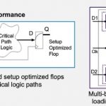
For their project, Qualcomm wrote the design rules that defined what the assembly should look like, including how to DRC and LVS comparisons on packages. Design rules had to be created that addressed package-specific requirements, including specifics such as size and distance of package wires. Figure 2 shows some typical design rule checks that might be included in an assembly design package.
STATS ChipPAC wrote rules for the TYPES of elements and configurations permitted in the package. This includes die-to-die edge, die-to-package edge, die-to-package alignment, corner rules, etc. Mentor’s role was to enhance the syntax in the Calibre® 3DSTACK tool to bring the two rule sets together and provide rule checking capabilities (Figure 3).
In assembly design kit LVS process, they used virtual die to test package layouts prior to assembly. The package doesn’t come with a netlist, but a spreadsheet “netlist” works well. This “netlist” format can contain electrical connection information as well as pin locations. By expanding Calibre 3DSTACK to support such formats, you can verify the routing connections in the package between die pins and BGA pins. It also enables the extraction of an assembly-level netlist, which, if used in conjunction with the process-specific chip LVS or PEX results, can be used to generate a full assembly-level netlist for feeding into downstream simulation and analysis tools.
Ferguson and Ramadan said the project went quite well, and they delivered the results in a session at DAC 2015. Using Calibre 3DSTACK, STATS ChipPAC created a rule file for their FOWLP process that can be used by any designer targeting this package technology at this assembly house, regardless of what processes the dies are, or how many dies are in the package. The rule file checks the manufacturing constraints of the package RDL and the die-to-die constraints, and verifies the connectivity through the package from die-to-die and die-to-BGA. It is entirely independent of any specific design tool used to generate the package.
The take-away message, Ferguson said, is that an assembly design kit provides a standardized process both chip design companies and assembly houses can use to ensure the manufacturability and performance of IC packages. This has been a gap in the IC supply chain. Using an assembly design kit can reduce risk of package failure, while also reducing turnaround time for both the component providers and assembly houses. By implementing a repeatable, proven process, all participants can improve both their first-time success rate and overall product quality.
Thanks to John Ferguson and Tarek Ramadan of Mentor Graphics.