In the spectrum of functional verification platforms – software-based simulation, emulation and FPGA-based prototyping – it is generally agreed that while speed shoots up by orders of magnitude (going left to right) ease of debug drops as performance rises and setup time increases rapidly, from close to nothing for simulation to days or weeks for prototypes.
All of this adds up to a real headache for debug in prototyping. While FPGAs provide some level of built-in logic analysis, these devices are designed primarily for optimal mission-mode performance, not for broad and deep debug. Which means that typically you have to instrument the design RTL with logic to bring out the signals you want to probe. So if you find a bug in one run, then guess exactly the right signals to probe and when to trigger to find the root-cause, re-instrument and re-run, you have managed to track down the problem with just one re-spin. More commonly you’re going to re-spin multiple times to converge on the right probe and trigger set. A Wilson Research Group/Mentor Graphics survey found prototyping teams took 4-6 re-spins on average to converge on a root cause for a bug. And you’re burning a lot of unproductive time on each re-spin. Or not if you feel the need to polish your sword fighting skills from the perilous heights of your trusty office chair 😎
I’m going to talk about Mentor’s solution to this problem, but first I should touch on something that had me puzzled for a while. Mentor doesn’t have their own prototyping box (that I know of), so why are they providing solutions in this space? In fact, they offer a software product called Certus for instrumenting FPGA-based designs, which they acquired from Tektronix around 2013. Tek had been working closely with the Dini Group (among others) and that relationship continues with Mentor. Since the Dini Group is very well known for building high-performance multi-FPGA boards, frequently used in prototyping, the pieces came together for me. Mentor through Certus, offers a solution for instrumenting custom multi-FPGA prototype boards, a commonly used platform today and likely into the future, especially in performance-driven applications.
Now back to the debug problem. A prototype for a large design may be split across multiple FPGAs, so a root-cause for a problem appearing in one FPGA could be in another FPGA. Then you have to worry about overhead for tracing signals. The most obvious approach, to add logic and wiring to probe each signal you might want to observe, quickly gets out of hand. Certus has a more efficient method. You can map up to 64K signals into an observability network with low overhead (~1 LUT per signal instrumented). The observability network is connected to a capture station which can capture traces from up to 1024 of these signals.
Which 1024 signals are captured can be reconfigured without needing to re-instrument and recompile the design. And you can have up to 255 capture stations per FPGA, so you can have a very high level of configurable visibility across all FPGAs on your prototype board, without need for recompiles. Capture stations store traces in ring buffers (controlled by user-defined triggers) which are efficiently compressed to store traces in on-FPGA memory. This approach can store up to seconds of trace-depth, up to 15 seconds in one example cited where bus activity related to an Ethernet MAC activity was being traced.
Or you can stream trace data to external memory. In another example cited, all activity was traced on an AXI bus in an A7-processor-based design during Linux boot, into a 4GB DDR memory, though Steve Bailey noted that there is some expected blanking during streaming, unless you are willing to enable pausing the design clocks during streaming. However, even when there is blanking correct ordering/causality between signals will be preserved. In fact this is generally ensured, across all clock domains and across all FPGAs. Where clocks are derived from the same crystal, signals within those domains are guaranteed to be correlated. If they are from different crystals, they may be off in correlation by one or two cycles but hey, Mentor can’t control relative drift in crystals. All of this correlation is ensured by Certus.
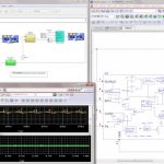
Visualizer debug pulls all of this together for detailed analysis. You drill down and trace back, as you do in debug. Maybe you decide you need to look at some traces you didn’t capture, so you need a new prototyping run, but now you probably don’t need to re-instrument. You just reconfigure some capture stations to add those traces. Of course it is possible that even with this flexibility you might have to re-instrument in some cases. But on-the-ground experience indicates that the original average 4-6 rebuilds drops to 0-1 rebuilds when using Certus.
Steve also mentioned that Certus supports reading out register states, though he acknowledges this requires stopping clocks and is quite slow. Still, he pointed out that once in prototyping, many users want to stay there as long as possible and will take an occasional slow operation in exchange for faster and deeper co-debug between hardware and software. You can learn more about Mentor support for FPGA prototyping debug HERE.