By Tetsu Ho
With the ever-increasing global demand for smarter, faster electronic systems, the semiconductor industry faces a dual challenge: delivering high-performance memory while reducing environmental impact. Winbond is meeting this challenge head-on by embedding sustainability into every layer of its operations—from green manufacturing processes to low-power memory innovations designed for AI, automotive, and industrial applications.
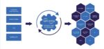
One of Winbond’s most significant innovations is its Customized Memory Solution (CMS)—a next-generation DRAM portfolio tailored for application-specific performance and power efficiency. Evolving from Winbond’s extensive DRAM heritage, CMS integrates advanced low-power architectures and 3D packaging like KGD 2.0 to meet the needs of edge AI, industrial automation, smart cities, and healthcare systems.
Green Manufacturing Starts at the Fab
Winbond’s fabrication site at Taichung, the Central Taiwan Science Park, is one of its most energy-efficient semiconductor facilities. Built with sustainability in mind, the Taichung Fab now operates on 90% renewable electricity, achieving a 60% reduction in carbon emissions compared to 2021. Its cleanroom and utility systems are optimized under the ISO 50001 energy management standard, while ISO 14064-1 and ISO 14067 certifications ensure accurate tracking of facility and product-level emissions.
Manufactured in Winbond’s green-certified fabs, CMS is an essential component of the company’s sustainable product strategy. Every CMS device benefits from a supply chain powered by 90% renewable electricity and is tracked through Winbond’s proprietary carbon accounting system, ensuring visibility of Scope 1, 2, and 3 emissions.
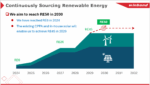
Winbond has committed to achieving RE50 by 2030, with half of its global energy consumption sourced from renewable sources. Its proprietary carbon inventory system accounts for Scope 1, 2, and 3 emissions, providing the company and its customers with clear visibility into environmental impact across the supply chain. This digital-first approach aligns with Taiwan’s carbon fee policy and prepares Winbond’s ecosystem for the rising demand for audited ESG data.
1.2V Serial NOR Flash: First in the Industry for Ultra-Low Voltage
Reducing system power begins at the component level. Winbond’s 1.2V Serial NOR Flash—the first in mass production—is a key step forward for energy-conscious design. This memory is built on a 45nm process, which significantly lowers active and standby power. It is ideal for battery-powered applications such as smart meters, wearables, and medical monitoring devices. This NOR Flash reduces the need for voltage regulators and extends battery life.
This enables designers to meet efficiency targets without compromising performance or reliability.
GP-Boost DRAM: High-Throughput, Low-Power Memory for Edge Intelligence
Winbond’s GP-Boost DRAM is designed for applications that require fast, continuous data processing at the edge, such as machine vision, real-time industrial control, or AI-enabled sensor hubs. Based on 20nm and advanced 16nm process nodes, it delivers high bandwidth and thermal stability while maintaining tight power budgets.
GP-Boost DRAM plays a key role in enabling real-time decision-making in embedded AI systems, without the need for active cooling or large energy reserves, making it a strong fit for both industrial and automotive markets.
CMS has already enabled a broad spectrum of intelligent systems—from motion control in factory automation and electric vehicle (EV) chargers, to secure medical devices, smart home systems, and AI-powered sensor hubs in smart cities. These deployments demonstrate how customized memory can extend device lifetime, reduce power draw, and support carbon reduction across vertical markets.
Octal and SLC NAND: Designed for Harsh Environments and Secure Performance
High-endurance Flash memory is essential in mission-critical systems, especially in automotive, industrial automation, and factory control applications. Winbond’s OctalNAND and SLC NAND Flash are built to withstand wide temperature fluctuations, intensive read/write cycles, and demanding performance requirements over long deployment periods.
Built-in bad block management, OTA (over-the-air) update support, and functional safety compliance help reduce failure rates and lower the environmental cost of field servicing or component replacement.
Embedded Security with Energy Efficiency: TrustME® Secure Flash
As embedded systems become more connected and vulnerable, data protection and sustainability are increasingly linked. Winbond’s TrustME® Secure Flash enables secure firmware storage, cryptographic key protection, and authenticated updates—all within a low-power profile optimized for edge and automotive environments.
By supporting secure OTA updates, Secure Flash helps extend device lifetime and reduces unnecessary physical servicing, ultimately lowering emissions and costs.
A Proven Commitment to ESG and Innovation
Winbond’s commitment to environmental, social, and governance (ESG) principles is embedded across its global operations—from how it sources raw materials to how it powers its fabs. Its sustainability performance has earned consistent external recognition, including the Taiwan Corporate Sustainability Awards (TCSA) ESG Award, the Corporate Sustainability Report Platinum Award, and a spot on the Top 100 Global Innovators list, acknowledging its technical leadership and responsible business practices.
A dedicated ESG Committee governs sustainability strategy, aligning with internationally recognized frameworks such as the Task Force on Climate-related Financial Disclosures (TCFD), the Responsible Business Alliance (RBA), and the Greenhouse Gas Protocol. The company publishes annual disclosures on emissions, energy use, and supply chain risk, including a Human Rights Due Diligence Report and a TCFD-aligned climate risk assessment.
Winbond’s environmental credentials are supported by third-party verified certifications, including but not limited to:
- ISO 14001 (Environmental Management Systems)
- ISO 14064-1 (Greenhouse Gas Emissions Inventory)
- ISO 14067 (Product Carbon Footprint)
- ISO 14046 (Water Footprint)
- ISO 50001 (Energy Management System)
- ISO 45001 (Occupational Health & Safety)
Winbond exceeds industry requirements by actively tracking Scope 3 emissions across its supply chain, utilizing its digital carbon accounting system. As a member of the Taiwan Climate Partnership (TCP), the company also works closely with other leading manufacturers to support shared decarbonization goals across the sector.
Whether switching to renewable energy early on or designing ultra-efficient memory products like the 1.2V Serial NOR Flash, GP-Boost DRAM, or CMS, Winbond is helping its customers reduce the carbon footprint of their end products. They’re shaping a more sustainable and resilient future for the semiconductor industry with a clear focus on transparency, measurable results, and practical action.
Conclusion: Sustainable Memory That Performs
Winbond’s sustainable semiconductor strategy is anchored in three core pillars: green fabs, green products, and green partnerships. By combining technical innovation with measurable sustainability gains, Winbond empowers OEMs and developers to create smarter, faster, and more environmentally responsible systems—from AI vision modules and electric vehicles to smart homes and industrial controllers.
Whether extending battery life, improving thermal performance, securing over-the-air updates, or ensuring environmental compliance, Winbond delivers the memory foundation for today’s high-performance, low-impact designs. Discover the complete portfolio at www.winbond.com.
Tetsu Ho, Technology Manager, holds a master’s degree in Industrial Engineering from National Tsing Hua University. He joined Winbond in 2005 and subsequently served as Product Engineer, Product Development Manager, and Marketing Technology Manager, and is responsible for promoting the EU DRAM market.
Also Read:
Sophisticated soundscapes usher in cache-coherent multicore DSP
Podcast EP297: An Overview of sureCore’s New Silicon Services with Paul Wells