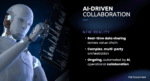
The PC industry is entering its most significant transformation since the debut of the IBM PC in 1981. That original beige box ushered in a new era of productivity, reshaping how corporations and individuals worked, communicated, and created. More than four decades later, the AI PC is emerging as a new category — one that promises to reignite growth in a market that has otherwise plateaued. Where the IBM PC democratized computing power for spreadsheets, word processing, and databases, the AI PC integrates machine intelligence directly into the device, enabling capabilities once reserved for cloud data centers.
“If the IBM PC made computers personal, the AI PC makes them perceptive”
What Defines an AI PC
An AI PC isn’t just another laptop or desktop with more cores or a faster GPU. At its heart lies a dedicated Neural Processing Unit (NPU) or an equivalent accelerator, designed to handle machine learning and inference tasks efficiently. Apple was among the first to bundle AI capability into all its Macs via the Neural Engine in its M-series silicon. In 2025, nearly all Macs shipped qualify as AI PCs by default. On the Windows/x86 side, Intel and AMD are racing to deliver NPUs in their latest laptop platforms, though only about 30% of PCs shipping this year meet the ‘AI PC’ definition. Meanwhile, RISC-V vendors are entering the scene with experimental AI PCs, such as DeepComputing’s DC-ROMA II, proving that even open architectures are chasing this category.
This hardware shift is paired with software integration. AI PCs promise not just raw horsepower but contextual, on-device intelligence. They run large language models (LLMs), generative tools, transcription, translation, and real-time personalization — all locally, without depending exclusively on the cloud.
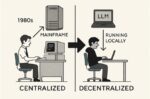
The IBM PC Parallel
The IBM PC, released in 1981, was revolutionary not because of its raw specs — an Intel 8088 processor, 16KB of RAM, and two floppy drives hardly impress today — but because of its timing and positioning. IBM gave business managers and knowledge workers their first taste of personal productivity at scale. VisiCalc and Lotus 1-2-3 spreadsheets became corporate staples, while WordPerfect transformed document workflows. The IBM PC became the catalyst for office automation and, eventually, the rise of the information economy.
The AI PC in 2025 carries a similar inflection point. Just as the IBM PC allowed managers to manipulate numbers without waiting for mainframe operators, the AI PC gives today’s professionals the power to run generative models, analyze vast data sets, and automate creative tasks directly from their desks. Where the IBM PC shifted power from IT departments to individual workers, the AI PC shifts power from centralized cloud servers back to the personal device.
How Apple Got the Jump on the x86 Crowd
Apple’s head start in AI PCs is the product of long-term bets that Intel and AMD were late to match. Apple began shipping a Neural Engine in iPhones as early as 2017. By the time the M1 arrived in Macs in 2020, Apple already had multiple generations of AI silicon in production. Intel’s first true NPU platform, Meteor Lake, didn’t appear until 2023, and AMD’s Ryzen AI chips landed around the same time.
Vertical integration gave Apple another edge. Because it controls silicon, operating system, and frameworks like Core ML and Metal, Apple can route workloads seamlessly across CPU, GPU, and NPU. The x86 ecosystem, fragmented between Microsoft, Intel, AMD, and dozens of OEMs, could not move nearly as fast.
Apple’s unified memory architecture offered a further advantage, eliminating costly data transfers that plague PCs where CPU and GPU have separate memory pools. And Apple made AI consumer-friendly: Apple Intelligence features in Mail, Notes, and Photos gave users visible, everyday value. Windows AI PCs, by contrast, still lean heavily on Microsoft’s Copilot features, many of which depend on cloud services.
By 2025, Apple had made AI hardware and features standard across its lineup. All Macs shipped are AI PCs, while only about a third of x86 PCs qualify.
The Day Apple Changed the Rules
The pivotal moment came at Apple’s Worldwide Developers Conference (WWDC) in June 2020. On stage, Tim Cook described it as a ‘historic day for the Mac’ and announced the company’s transition to Apple-designed silicon. He framed it as the next evolution in Apple’s decades-long control of its own hardware and software stack.
Johny Srouji, Apple’s Senior Vice President of Hardware Technologies, then took the stage to explain the architectural foundations of what would later be branded the M1. He described how Apple’s silicon journey — from iPhone to iPad to Apple Watch — had matured into a scalable architecture capable of powering Macs. Srouji highlighted the unification of CPU, GPU, and Neural Engine within a single system-on-chip, the adoption of a unified memory architecture, and a focus on performance per watt as the key to efficiency. He emphasized that Apple’s decision to design its own SoCs specifically for the Mac would give the platform a leap in power efficiency, security, and AI capability.
This keynote framed the M1 not just as a chip, but as the product of a strategic pivot — one that caught the x86 world by surprise and set Apple years ahead in the race to define the AI PC.
Inside Apple’s Secret AI Weapon
The Neural Processing Unit (NPU) in every modern Mac isn’t an ARM building block — it’s an Apple original design. Apple licenses the ARM instruction set for its CPUs but develops its own CPU, GPU, and NPU cores.
The Neural Engine debuted with the A11 Bionic in 2017, years before ARM’s Ethos NPU line, and has scaled up steadily to handle tens of trillions of operations per second. It was conceived and built in-house by Apple’s silicon team under Johny Srouji, tailored specifically for machine-learning inference. In the M1, the Neural Engine delivered 11 TOPS, while in the M3 it exceeds 35 TOPS.
The GPU inside the M1 was also a clean Apple design. Until the A10 generation, Apple licensed PowerVR graphics cores from Imagination Technologies, but starting with the A11 Bionic in 2017, Apple switched to its own custom GPU microarchitecture. The M1’s 8-core GPU, capable of 2.6 TFLOPS, is part of this lineage.
Taken together, Apple’s CPU, GPU, and Neural Engine represent a vertically integrated architecture — all custom, all Apple — with only the instruction set itself licensed from ARM. This tight ownership is what allows Apple to optimize across hardware and software, and it explains why the M-series has been able to leapfrog x86 designs in efficiency and AI capability.
Birth of The AI PC
Apple didn’t set out to build the M1 in 2010, but its path toward full integration began to take shape years earlier. When the company introduced its first in-house Neural Engine and custom GPU alongside its homegrown CPU in the A11 Bionic (2017), it effectively unified all three pillars of modern computation under one roof. From that point on, Apple’s silicon roadmap evolved with a clear long-term goal: to bring these independently perfected engines — CPU, GPU, and Neural Engine — onto a single fabric with shared memory and software control. The M1, unveiled in 2020, was the culmination of that decade-long convergence, transforming what had started as separate mobile components into a cohesive architecture optimized for both performance and efficiency across the entire Mac lineup.
While NVIDIA’s “aha moment” came in 2012, when its GPUs unexpectedly became the workhorses of the deep learning revolution, Apple was on a parallel but opposite trajectory. NVIDIA was scaling up for the cloud, harnessing GPU clusters for AI training, while Apple was scaling down — embedding intelligence directly into personal devices. Both arrived at AI through performance innovation rather than foresight: NVIDIA by discovering that its gaming chips excelled at matrix math, and Apple by realizing that machine learning could make mobile experiences smarter, faster, and more private. The convergence of these two paths — one born in the data center, the other in the palm of the hand — defined the modern era of AI computing.
Competing Compute Models—Apple vs. RISC-V
Apple’s M-series SoCs represent a tightly integrated approach. At the CPU level, Apple uses a combination of high-performance and efficiency cores, delivering strong single-thread performance while managing orchestration tasks at low power. Its GPU, designed in-house, is a tile-based architecture that handles both graphics and general-purpose compute. For AI-specific workloads, Apple includes its Neural Engine, a dedicated block capable of roughly 35 TOPS in its latest Macs, deeply integrated with Core ML and Apple Intelligence. Together, these components form a unified architecture with shared memory, which eliminates costly data transfers and optimizes performance for consumer-facing AI applications.
RISC-V vendors, by contrast, take a modular approach based on scalar, vector, and matrix engines. Scalar cores serve as the foundation for control and orchestration, while the RISC-V Vector Extension (RVV 1.0) provides scalable registers ranging from 128 to 1024 bits, ideal for SIMD tasks like convolution, dot-products, and signal processing. For high-intensity AI workloads, matrix engines (MMA) accelerate tensor math in formats such as INT8, FP8, and FP16, targeting operations like GEMM and transformer attention. Rather than a closed design, this modular architecture allows vendors to tailor solutions to specific needs and even adopt chiplet-based scaling across regions and partners.
The contrast between Apple and RISC-V is sharp. Apple delivers a closed but seamless integration, while RISC-V offers openness, extensibility, and flexibility. Apple’s ecosystem is polished and tightly controlled, with Core ML and Apple Intelligence driving user-facing features. RISC-V, on the other hand, still relies on maturing toolchains like LLVM, ONNX, and TVM, but its open model makes it attractive for sovereign compute initiatives and experimental AI PCs. Apple scales its approach within its own lineup, while RISC-V enables innovation across global vendors, offering a pathway that Apple’s ecosystem simply does not allow.
Why the x86 Crowd Got Caught Flat-Footed
The x86 ecosystem misjudged both the timing and the scope of the AI PC transition. For years, Intel and AMD assumed that AI workloads would remain concentrated in data centers and GPUs rather than extending into consumer PCs. Their product roadmaps and marketing focused on server accelerators and high-performance gaming graphics, while NPUs for laptops were treated as an afterthought.
This miscalculation was compounded by the industry’s preoccupation with the data center boom. As hyperscalers poured billions into AI infrastructure, chipmakers directed their attention toward GPUs and server CPUs, chasing growth where the margins were highest. In doing so, they overlooked the parallel opportunity Apple had identified — embedding AI into personal devices where privacy, latency, and convenience are paramount.
By the time Intel released Meteor Lake in 2023 and AMD introduced Ryzen AI, Apple already had a three-year head start in consumer AI integration. Microsoft’s Copilot+ PC initiative in 2024 only underscored how reactive the x86 response had become. Moreover, Intel’s manufacturing struggles and AMD’s limited focus on NPUs slowed their ability to pivot, while power efficiency remained a glaring weakness. Apple could deliver hours of local LLM performance on battery, something x86 laptops could not match without resorting to power-hungry discrete GPUs.
Ultimately, the fixation on data centers blinded x86 vendors to the rise of the AI PC. Apple exploited this gap decisively, while RISC-V vendors now see an opportunity to carve out their own space with modular, integrated solutions that offer an open alternative to both Apple and x86.
NVIDIA’s Head is in The Cloud
NVIDIA dominates AI in the cloud and remains the gold standard for GPU-accelerated training and inference. Its CUDA ecosystem, TensorRT optimizations, and developer lock-in make it indispensable in enterprise and data center environments. But the AI PC revolution is shifting focus toward efficient, always-on AI computing at the edge, and here NVIDIA plays a more complicated role.
On the one hand, NVIDIA powers some of the most capable ‘AI PCs’ today. Discrete RTX GPUs deliver blazing inference speeds for LLMs and generative models, and Microsoft has partnered with NVIDIA to brand ‘RTX AI PCs.’ For power users and creators, an x86 laptop with an RTX 4090 GPU can churn out tokens per second far beyond what Apple’s Neural Engine can achieve.
On the other hand, NVIDIA’s model depends on discrete GPUs that consume far more power than Apple’s integrated NPUs or the NPUs Intel and AMD are embedding into CPUs. AI PCs are not just about raw throughput — they are about balancing performance with efficiency, portability, and battery life. Apple has made AI capability universal across its product line, while NVIDIA’s approach is tied to high-end configurations.
This leaves NVIDIA both central and peripheral. Central, because any developer serious about AI still needs NVIDIA for training and high-performance inference. Peripheral, because the AI PC category is being defined around integrated NPUs, not discrete GPUs. If ‘AI PC’ comes to mean a lightweight laptop with always-on AI features, NVIDIA risks being left out of the mainstream narrative, even as it continues to dominate the high end.
Apple’s Big Mac: The Comeback Story
After two decades in the iPhone’s shadow, the Mac is regaining its relevance — not as a nostalgia act, but as the world’s first mass-market AI PC. The AI PC wave also reshapes Apple’s internal dynamics. For nearly two decades, the iPhone was Apple’s growth engine, overshadowing the Mac. iPhone revenue reached more than $200 billion annually, while the Mac hovered around $25–30 billion. The company’s focus, culture, and ecosystem tilted toward mobile.
But smartphones are now a mature market. Global shipments have flattened, replacement cycles lengthened, and Apple increasingly leans on services for growth. The iPhone remains indispensable, but its role as the company’s primary driver is fading.
The Mac, reborn as the AI PC, offers Apple a chance to regain strategic balance. AI workloads — text generation, media editing, data analysis — naturally fit the desktop and laptop form factor, not the smartphone. Apple Intelligence on the Mac positions it as an AI hub for professionals, creators, and students, in ways the iPhone cannot match due to thermal and battery constraints.
This doesn’t mean the Mac will replace the iPhone. Instead, Apple could emerge as a two-pillar company: the iPhone for mobility, and the Mac for intelligence. For the first time in 20 years, the Mac may outpace the iPhone in growth, reclaiming relevance and giving Apple a new narrative.
Why the Market Needs Reignition
| AI PC Shipments, Worldwide, 2023-2025 (Thousands of Units) |
|
2023 Shipments |
2024 Shipments |
2025 Shipments |
| AI Laptops |
20,136 |
40,520 |
102,421 |
| AI Desktops |
1,396 |
2,507 |
11,804 |
| AI PC Units Total |
21,532 |
43,027 |
114,225 |
| Source: Gartner (September 2024) |
|
|
The global PC market has stagnated for years, with shipments hovering between 250 and 300 million units annually. Upgrades slowed as performance improvements became incremental, and consumers extended replacement cycles. But AI is creating a new reason to buy. Gartner projects AI PC shipments will grow to about 114 million units in 2025 — a 165 percent increase over 2024 — representing more than 40 percent of the entire PC market. That figure is expected to rise sharply as AI features become standard in both macOS and Windows, echoing how spreadsheets once drove mass PC adoption.
Apple has tightly coupled its Apple Intelligence software features with the Neural Engine in its Macs, positioning every new Mac as an AI PC. Microsoft is building its Copilot assistant into Windows, with hardware requirements that virtually guarantee demand for NPUs in next-generation x86 machines. Even RISC-V, still a nascent player in consumer computing, is positioning AI PCs as a proving ground for its open ISA.
Corporate and Individual Drivers
The IBM PC spread through corporations first. Executives and managers demanded their own productivity machines, which soon became indispensable for day-to-day decision-making. A similar pattern is emerging with AI PCs. Corporations now view them as essential tools for efficiency, where sales teams can generate proposals on demand, analysts can automate reporting, and creative departments can accelerate design and media production. Buying an AI PC for every employee is becoming the new baseline for productivity, much like issuing a PC to every manager was mandatory in the 1980s.
At the same time, individuals are also driving adoption. Students, freelancers, and creators are eager to run local language models for research, content generation, and coding without being tethered to cloud subscriptions. Emerging players such as DeepComputing, in partnership with Framework, are helping expand access to RISC-V–based AI PCs designed for developers and open-source enthusiasts who want full control over their hardware and software stack. Just as early home PCs became invaluable to small business owners and families, today’s AI PCs are rapidly evolving into indispensable personal assistants.
Challenges and Opportunities
As with the IBM PC era, the rollout of the AI PC comes with challenges. Software ecosystems must catch up, ensuring that frameworks like PyTorch, TensorFlow, and ONNX can fully exploit NPUs across different architectures. Pricing remains a consideration as well. Macs with integrated NPUs begin at around $1,099, while x86-based AI PCs often carry higher costs, and RISC-V systems remain experimental and relatively expensive.
Despite these hurdles, the opportunities are far greater. The AI PC offers a compelling reason to refresh hardware and injects new vitality into a stagnant market. It has the potential to redefine productivity just as spreadsheets once did in the 1980s. The modern equivalent of the spreadsheet ‘killer app’ may well be the personal AI assistant — a ubiquitous capability that transforms how individuals and corporations alike work, learn, and create.
“Copilot isn’t the killer app the AI PC needs. That breakthrough will come when on-device AI stops looking to the cloud—and starts thinking for itself.”
Conclusion
The AI PC in 2025 echoes the IBM PC in 1981: a new category that redefines what personal computing means and who benefits from it. The IBM PC turned the desktop into a productivity hub. The AI PC transforms it into a creativity and intelligence hub.
Apple is the clear frontrunner in this takeoff. Years of NPU integration, vertical stack control, unified memory, and seamless software have given it a commanding lead. The x86 vendors were caught flat-footed not only by ecosystem fragmentation and roadmap delays, but also by their tunnel vision on data centers. NVIDIA, meanwhile, remains the giant in cloud AI and the supplier of the fastest PC accelerators, but it risks being sidelined in the volume AI PC market if integrated NPUs become the standard definition.
For Apple, this represents more than just an industry lead. It signals the Mac’s return as a growth engine at a time when the iPhone’s dominance is beginning to plateau. If history is any guide, this shift will not just reinvigorate PC shipments but will reshape the role of the computer in society — making the AI PC the defining tool of the next era in computing.
Also Read:
GlobalFoundries, MIPS, and the Chiplet Race for AI Datacenters
Yuning Liang’s Painstaking Push to Make the RISC-V PC a Reality
Rapidus, IBM, and the Billion-Dollar Silicon Sovereignty Bet


![[white paper] Parasitic Analysis Figures](https://semiwiki.com/wp-content/uploads/2025/10/Fig1-net-level-visualization-150x127.jpg)