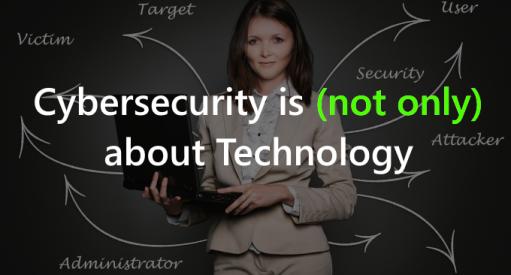
RVN! 26 Banner revised (800 x 100 px) (600 x 100 px)

Emulation makes the What to See List

Emulation makes the What to See List
by Daniel Payne on 07-25-2017 at 12:00 pm

The analysts at Gary Smith EDA produce an annual What To See List for DAC and I quickly noticed that all three major EDA vendors were included on the list for the specific category of emulation. The big problem that emulation addresses is the ability to run in hardware an early version of your SoC so that software developers can get access and run lots of code or boot an OS, plus the hardware team can more quickly verify and debug the performance of their system to see that it will meet all specifications prior to first silicon. On the Wednesday at DAC I was able to watch a booth discussion at Mentor where Samsung, ARM and Starblaze engineers talked about their emulation experiences, moderated by Lauro Rizzatti.

The three panelists were:

  • Rob Kaye, ARM
  • Nasr Ullah, Samsung
  • Bruce Cheng, Starblaze

Q&A

Q: There is In-Circuit Emulation mode and Virtual deployment mode for emulation. Which emulation use model have you tried and why?

A: Samsung – we are using emulation in three areas: Performance, are the projections correct? Did our implementation meet the requirements? Can we add a late feature? Our team needs to verify that the quality of service is sufficient so that they can make a phone call along with streaming video on a mobile device. Emulation helps us with meeting the power constraints, knowing that the chip runs cool enough and that the current levels fit the battery.

A: Starblaze – we need to run our real application firmware on the SSD controller. We have a PCIe connection in order to match the speed of our host. The NAND interface is affected by aging. We’re using 100% virtual peripherals with the VirtuaLAB toolkit, where PCIe is virtual and a simulator connects to the emulator through DPI (Direct Programming Interface).

The PCIe PHY in our ASIC is modeled with a virtual PCIe PHY in emulation. On the NAND interface we use fast memory models running on the host, making simulation fast. This is a pure virtual approach and allows us to change configurations, or system performance

A: ARM – both our IP validation and IP development teams use emulation. Our SW group does early development with virtual prototypes, the move key parts into emulation to run SW at a fully-timed level. Software-driven validation is another approach used where virtual and emulation combine to allow C code to run on the CPU model while debugging drivers and we develop validation flows for parts on the emulator.

Related blog – Listening to Veloce Customers: Emulation is Thriving

Q: Describe a verification challenge and how emulation came to the rescue.

A: Samsung – we had our design running in emulation, after four days of running Android and apps the performance slowly declined. Emulation uncovered a counter bug where the counter didn’t reset. Simulation would never have found that bug.

A: Starblaze – an application in our ASIC would run for five days then crash. We ran the modified application in our emulator to trace and debug the problem. Prototypes have been built with FPGAs, however they provide little visibility inside to help with debug and recompile times can be 10 hours or longer, so with emulation we have more convenient debugging.

A: ARM – running GPU benchmarks is sped up with emulation.

Q: Any recommendations to emulation users or vendors?

A: Samsung – start your emulation as early as possible. Have verification engineers start early with emulation in order to find and fix more issues.

A: Starblaze – emulation vendors need to make them run faster, because we’re not as fast as the ASIC yet. Keep improving and adding debug tools like VirtuaLAB PCIe. Would love a NAND or CPU analyzer.

A: ARM – we want context switching between virtual and emulator and then run to some point in the simulator or emulator.

Related blog – The Rise of Transaction-Based Emulation

Q: Will emulation be here in five years and will it be different?

A: Samsung – I like what ARM asked about context switching. We can run high-level simulation and mix/match it with emulation. We need the ability to switch between lower design details and the highest abstraction layer.

A: Starblaze – Our customers use a behavioral model of the chip to run firmware, it’s an SSD simulator. We want to link the SSD simulator to the emulator and be able to switch context. Verification is moving to higher levels of abstraction, so emulation has to follow that trend.

A: ARM – we see emulation being used in SW/HW integration for SW regression testing. Embedded software has grown in size, even Android uses about 20 billion instructions. Emulation lets us run lots of these tests of our software for both function and performance. More of our software development teams will use emulation in the future.

Related blog – Mentor Plays for Keeps in Emulation

Summary
After the panel questions concluded I did ask my own question, “Are you using other vendor emulators?”

Both Samsung and ARM replied yes, while Starblaze only uses the Mentor emulator.

Perhaps it is time for your group to consider using an emulator on the next SoC project and start getting the same kind of benefits that ARM, Samsung and Starblaze reported seeing in their design and verification flows.


Virtualizing ICE

Virtualizing ICE
by Bernard Murphy on 07-25-2017 at 7:00 am

The defining characteristic of In-Circuit-Emulation (ICE) has been that the emulator is connected to real circuitry – a storage device perhaps, and PCIe or Ethernet interfaces. The advantage is that you can test your emulated model against real traffic and responses, rather than an interface model which may not fully capture the scope of real behavior. These connections are made through (hardware) speed bridges which adapt emulator performance to the connected device. And therein lies (at times) a problem. Hardware connections aren’t easy to virtualize, which can at times impede flexibility for multi-interface and multi-user virtual operation.


A case of particular interest, where a different approach can be useful, arises when the “circuit” can be modeled by one or more host workstations; where say multiple GPUs modeled on the emulator may be communicating through multiple PCIe channels with host CPU(s). Cadence now supports this option through Virtual Bridge Adapters for PCIe. This is a software adapter, allowing OS and user applications on a host to establish a protocol connection to the hardware model running on the emulator. As is common in these cases, one or more transactors running on the emulator manage transactions between the emulator and the host.

I wrote about this concept earlier in a piece on transaction-based emulation, but of course a general principle is one thing – a fully-realized PCIe interface based on this principle is another. This style of modeling comes with multiple advantages: low-level software can be developed/debugged against pre-silicon design models, this style can support multiple users running virtualized jobs on the emulator and users can model multiple PCIe interfaces to their emulator model. Also, and this is a critical advantage, the adapter provides a fully static solution. Clocks can be stopped to enable debug/state dump or to insert faults without the interface timing-out, something which would be much more challenging with a real hardware interface.


Frank Schirrmeister pointed out how this fills a verification IP hole in the development flow. In IP and subsystem development, you’ll validate protocol compliance against simulation VIPs or accelerated equivalents running on an emulator. When you want high confidence that your design behaves correctly in a real system handling real traffic, you’ll use an ICE configuration with speed-bridges. In-between there’s a place for virtual emulation using virtual bridge adapters. In the early stages of system development, there’s a need to validate low-level software (e.g. drivers) for those external systems, before you’re ready to move to full ICE with external motherboards and chipsets. Modeling using virtual bridge adapters provides a way to support this.

Frank offered two customer case-studies in support of this use model. Mellanox talked at CDNLive in Israel about using virtual adapters and speed bridges in a hybrid mode for in-circuit-acceleration (ICA). They indicated that this provides the best of both worlds – speed and fidelity in the stable part of the system circuit and flexibility/adaptability in software development and debug for evolving components.

Nvidia provided a more detailed view of how they see the role of ICE and virtual bridging. First for them there is no question that (hardware-based) ICE is the ultimate reference test platform. They find it to be the fastest verification environment, proven and ideal for software validation and it has the flexibility and fidelity to test against real-world conditions, notably including errata (something that might be difficult to fully cover in a virtual model). However, applying only this approach is becoming more challenging in the development phase as they must deal with an increasing number of PCIe ports, more GPUs and more complex GPU/CPU traffic, along with a need to support new and proprietary protocols.

For Nvidia, virtual bridge adapters provide help in emulation modeling for these needs. Adding more PCIe ports becomes trivial since they are virtual. They can also provide adapters for their own proprietary protocols and support both earlier versions and the latest revisions. As mentioned above, the ability to stop the clock greatly enhances ease of debug while in development. At the same time Nvidia were quick to point out that virtual-bridge and speed-bridge solutions are complimentary. Speed bridges give higher performance and ensure traffic fidelity. Virtual bridges provide greater flexibility earlier in the development cycle. Together these fill critical and complementary needs.

The big emulation providers have at times promoted ICE over virtualization or vice-versa; perhaps unsurprisingly the best solution now looks a combination of both solutions. As always, customers have the final say. You can watch Nvidia’s comments on the Palladium-based solutions HERE.


Seeking Autonomy

Seeking Autonomy
by Tom Simon on 07-24-2017 at 12:00 pm

I’d wager that if I mention autonomous vehicles, the first thing that you would think of would be autonomous cars. The truth is that we will see many other kinds autonomous vehicles in the years ahead. Their applications will range from package delivery to saving lives on the battlefield. Of course, to some extent they are already used on the battle field for less than benevolent purposes.


We have heard that Amazon is experimenting with the idea of package delivery using drones. Their Prime Air service is already delivering packages within 30 minutes in England. Their website features several videos of the service operating today. They have even gone so far as to watermark the videos with “Not Simulated”. The drones they are using fly presently only in clear weather and at an altitude of 400 feet.

Another fascinating application for autonomous vehicles in battlefield rescue. The army has been working on this for over a decade. The system most talked about is called BEAR for Battlefield Extraction Assist Robot. While these are not going to be fully autonomous they will be able to receive commands and execute them with some degree of autonomy. An interesting human engineering aspect of the rescue robots is that it was discovered that solders felt vastly more comfortable with robots that look less mechanical and more lifelike. The prototypes have faces and appendages that look like arms. Yet the propulsion mechanisms are hardly anthropomorphic and are highly optimized for moving over rough or uneven terrain.

The final category of autonomous vehicles I want to touch upon is flying cars. In March it was reported that Dubai is planning to offer autonomous airborne taxis service. They are going to be using the Ehang 184 which is being developed in China. It can carry one person with 8 rotors on 4 arms, thus ”184”. Pilotless air flight raises many questions about safety and practicality. Nevertheless, it seems that we are headed in that direction and it is only a matter of time. In congested urban areas, autonomous flying taxis would be highly sought after.

I am sure in reading above about the potential applications for autonomous vehicles that reliability and safety are the two things that immediately come to mind. It’s not hard to image many potential sources of errors, causes of failures and other factors that could cause safety and reliability issues. Sidense has been talking about security and reliability for autonomous systems for quite a while. Their non-volatile memory (NVM) can help contribute to improved reliability and safety in a number of ways. It’s important to understand the role that NVM can play in these systems.

NVM is used to store boot code, encryption keys, trim information, unique identifiers and many other sorts of critical information. System design requirements often dictate constraints on area, power, process technology, and durability. Instead of adding off chip NAND flash or resorting to exotic processes for storing mission critical information, Sidense One Time Programmable (OTP) NVM uses minimal real estate and can be implemented inside SOC’s on standard planar and FinFET processes. It also offers impressive durability due to its uniquely designed 1-T bitcell. In fact, it can tolerate extremely harsh operating environments.

Data stored with Sidense OTP NVM is extremely secure. There is no way to physically examine the silicon to determine its contents. The write operation causes atomic level disruption to the oxide layer that is impossible to detect through mechanical or visual means. Reverse engineering is thwarted by numerous features that defeat techniques like side channel attacks or other electronic hacking.

Designers of autonomous systems are pushed to meet multiple and potentially mutually exclusive design goals. At every step in the design process conflicting criteria and objectives need to be balanced. It’s good that for many NVM needs in these systems there is a robust, reliable, secure and low overhead solution. Sidense works with foundries to develop comprehensive qualification reports and information to ensure that their technology works well within spec. If you want to learn more about how Sidense OTP NVM can be applied to demanding applications like autonomous vehicles, I recommend looking at their published article on their website.


The Transformation of Silvaco!

The Transformation of Silvaco!
by Daniel Nenni on 07-24-2017 at 7:00 am

Founded in 1984, Silvaco is now the largest privately held EDA company with a rich history including a recent transformation that is worth a blog if not a book. Coincidently, I started my career in Silicon Valley in 1984 and have had many dealings with Silvaco over the years including a personal relationship with Silvaco founder Ivan Pesic. The transformation I am speaking of started when David Dutton became CEO in 2014 and covers the last three years. They joined SemiWiki in 2013 so we have had a front row seat.

You can see a brief history of Silvaco on SemiWiki HERE. Interestingly, the views on this blog are comparable to the views on the brief history of Cadence, Synopsys, and Mentor blogs. You can also read the CEO interview we did in January with David HERE. This was also a well-read blog.

David and I are on the same page with the transformation EDA is currently undergoing. Semiconductor design is getting harder with each new node and with fabless systems companies in the mix, time-to-market pressures continue to compress the design cycle forcing EDA customers to focus on a much smaller number of vendors. It is called a “fewer throats to choke when something goes wrong” strategy. Given that, take a look at the acquisition spree Silvaco has gone on in the last two years:

Silvaco to Acquire SoC Solutions
(June 16th, 2017)

Silvaco Accelerates Characterization Business with Agreement to Acquire Paripath
(June 14th, 2017)

Silvaco Enters IP Market With Acquisition of IPextreme
(June 3rd, 2016)

Silvaco Group Acquires edXact for SPICE Simulation Speed-up
(June 2nd, 2016)

Silvaco Extends SPICE Product Portfolio to Address Advanced Variation-Aware Design with Acquisition of Infiniscale
(December 15th, 2015)

Silvaco Acquires Invarian to Accelerate Adoption of Concurrent Power-Voltage-Thermal Analysis
(March 19th, 2015)

This month they launched a worldwide series of SURGE events. SURGE stands for Silvaco UserRs Global Events which shows the company’s commitment to expanding their customer base.

“Our inaugural Silvaco UseRs Global Event, SURGE, in Hsinchu Taiwan exceeded our expectations with strong attendance and user participation. The keynote speech on PixelLED Development by Dr. Charles Li, CEO of Playnitride, was well received by the audience showing the challenges of leading-edge LED display design. The power of bringing our technology experts to our users is a further step in Silvaco’s commitment to provide solutions to our customers for their ever-increasing challenges in display and semiconductor design. We are looking forward to hosting SURGE’s worldwide user base throughout 2017 and to building them stronger in the years ahead.”David Dutton, CEO of Silvaco.

These types of gatherings are what makes EDA great, the ability to collaborate directly with the people who use the tools, absolutely. Be sure and check the schedule and attend the one closest to you. I will be at the one in Silicon Valley and it would be a pleasure to meet you!

About Silvaco, Inc.

Silvaco, Inc. is a leading EDA provider of software tools used for process and device development and for analog/mixed-signal, power IC and memory design. Silvaco delivers a full TCAD-to-sign-off flow for vertical markets including: displays, power electronics, optical devices, radiation and soft error reliability and advanced CMOS process and IP development. For over 30 years, Silvaco has enabled its customers to bring superior products to market with reduced cost and in the shortest time. The company is headquartered in Santa Clara, California and has a global presence with offices located in North America, Europe, Japan and Asia.


Webinar: Ansys on Multi-Physics PDN Optimization for 16/7nm

Webinar: Ansys on Multi-Physics PDN Optimization for 16/7nm
by Bernard Murphy on 07-22-2017 at 12:00 pm

On the off-chance you missed my previous pieces on this topic, at these dimensions conventional margin-based analysis becomes unreasonably pessimistic and it is necessary to analyze multiple dimensions together. People who build aircraft engines, turbines and other complex systems have known this for quite a long time. You can’t analyze fluid dynamics, temperature and mechanical factors separately against margins on the other factors, at least not if you to want to build competitive solutions.


REGISTER NOW for this webinar at 8:00am PDT on August 3rd

Guess what – we now have a similar problem; important dimensions for semiconductor design are somewhat different but, at 16nm and below, just as multi-faceted, as design teams are already finding in significant deltas between margin-based analyses and multi-physics analyses. The margin-based approach analyzes timing, for example, with margins on operating voltage. But increased power-noise sensitivity as operating voltages get closer to threshold voltage (as they do in these advanced technologies) can cause nominally safe critical paths to fail both thanks to increased path-delay and clock jitter.

Margining this away becomes impractical – why should the whole PDN pay for one unusually large power dip in one use-case in one part of the circuit? Conversely, how do you know you didn’t miss that power dip in one otherwise unremarkable simulation while building your margins?

Ansys will talk about their SeaScape-based approach through big data analytics and elastic compute technology to enable multi-physics analysis and solve this problem the right way. Big data and elastic compute is an emerging wave in design. You might want to check it out.

REGISTER NOW for this webinar at 8:00am PDT on August 3rd

Ansys Summary
Next-generation automotive, mobile and high-performance computing systems demand the use of 16/7nm SoCs that are bigger, faster and more complex than ever. For these SoCs, the margins are smaller, schedules are tighter and costs are higher. Faster convergence with exhaustive coverage is imperative for on-time silicon success. The growing interdepencies among various multiphysics attributes such as timing, power and thermal properties in N16/N7 designs poses significant challenges for design closure. Existing solutions are not architected to solve for such a multidimensional optimization problem.

Join us for this webinar to learn how to maximize design coverage and accelerate convergence for SoC power signoff using the latest ANSYS SeaScape platform in big data systems. With unparalleled scalability across hundreds of cores using big data techniques, SeaScape helps you sign off on 1 billion+ instance designs within a few hours on commodity hardware. You will also learn how you can leverage multivariable analytics to achieve significantly better signoff confidence and drive meaningful design optimization.


Does Elon Musk Hate Artificial Intelligence?

Does Elon Musk Hate Artificial Intelligence?
by Matthew Rosenquist on 07-22-2017 at 7:00 am

Elon Musk, the tech billionaire and CEO of Tesla, was quoted as saying Artificial Intelligence (AI) is the “Greatest Risk We Face as a Civilization”. He recently met with the National Governor’s Association and advocated for government involvement and regulations. This seems to be a far cry from the government-should-leave-the-market-alone position high-tech firms normally advocate. At first glance, it seems awkward. The head of Tesla, who has aggressively invested in AI for self-driving cars, is worried about AI and wants bureaucratic regulation?

Is Musk driven by unwarranted fear or possibly taking this brash position as part of a marketing stunt? What is he actually saying? Well, I think he is being rational.

Translating Technology Fear
Mr. Musk is a brilliant technologist, engineer, and visionary (I am a fan of his work). I have never sat down and had a chat with him, but from what I have understand, his concerns seem informed and grounded, as they would for any technology that has great power. AI will bring tremendous value and will extend computing beyond just analysis of data, to manifest in the manipulation of the physical world. Autonomous transportation is a great example where AI will enable vehicles to eventually be in total control. Therefore, life-safety of passengers and pedestrians will be in the balance.

History teaches many lessons. Alfred Nobel’s invention was revolutionary in fueling the global industrial and economic revolutions. It was designed to accelerate the mining of resources and building of infrastructure while improving the safety during transport and use. Ultimately, to Nobel’s displeasure, it was also used as the preferred compound for destruction and taking lives in wars across the globe.

More recently, advances in genetics emerged with the potential of medical breakthroughs and sweeping cures for afflictions that cause massive suffering. But again, such power could be misused and result in unintended consequences (destruction of our species, ravaging planetary ecosystems, etc.). Scientists and visionaries spoke up over a decade ago to support controls that throttled certain types of research. Such regulations and oversight has given the world time to understand certain ramifications and be more cautious as it moved forward with research.

Race to Destruction

Business competition is fierce and the race for innovation often casts aside safety. Government involvement can slow down the process, to allow more attention to avoid catastrophes and for society to debate the right level of ethical standards.

There was little need to argue for the regulations to be enacted to control the research and development of chemical, biological, and nuclear weapons. It was obvious. Nobody wants their neighbor to be brewing anthrax in their bathtub. But for cases where the risks are not apparent and potentially obscured by the great benefits, it becomes more problematic. Marie Curie, the famed chemist made great advances to modern medicine, with little regulatory oversight, and ultimately died from her discoveries. Nowadays, we don’t want just anyone playing around with radioactive isotopes. There is government oversight. The same is true for much of the medical and pharmaceutical world where research has boundaries to keep the population safe.

Artificial Intelligence, aside from science fiction movies where computers become self-aware and attempt to destroy mankind, is vague. It can encompass so much, but still be difficult to describe exactly what it can and cannot do. This is where technology visionaries play a role. Some have a keen insight to see the risks. Elon Musk, Stephen Hawking, and Bill Gates have also discussed publicly their concerns for runaway AI.

“AI’s a rare case where we need to be proactive in regulation, instead of reactive. Because by the time we are reactive with AI regulation, it’s too late,”– Elon Musk


Innovation and Caution

I believe Musk wants to raise awareness and establish guard-rails to make sure innovation does not recklessly run-away at the detriment of safety, security, and privacy. He is not saying AI is inherently bad. It is just a tool. One which can be used benevolently or with malice, and runs the risk of mistakenly being wielded in ways that create severe unintended consequences. Therefore, his message to legislators is that we must respect the power and move with more forethought as we improve our world.

Interested in more? Follow me on LinkedIn, Twitter (@Matt_Rosenquist), Information Security Strategy, and Steemit to hear insights and what is going on in cybersecurity.


Semicon West – The FDSOI Ecosystem

Semicon West – The FDSOI Ecosystem
by Scotten Jones on 07-21-2017 at 12:00 pm

At Semicon West last week I attended presentations by Soitec and CEA Leti, and had breakfast with CEA Leti CEO Marie Semeria, key members of the Fully Depleted Silicon On Insulator (FDSOI) ecosystem. I have also seen some comments in the SemiWiki forum lately that make me believe there is some confusion on the roles of different companies in the FDSOI ecosystem. In this article, I will review the key players and their roles and then discuss the latest updates.

FDSOI Ecosystem
Figure 1 illustrates the roles of the major players in the FDSOI ecosystem.


Figure 1. The FDSOI ecosystem.

Regardless of whether a process is bulk, FDSOI or FinFET all of the major companies running wafer fabs buy the starting substrates. For FDSOI, an SOI wafer is needed with a thin silicon devices layer over a thin buried oxide layer. The leading provider of FDSOI wafers is Soitec with SEH as a licensed second source.

The fab operators for FDSOI are ST Micro as an Integrated Device Manufacturer (IDM) and Samsung and GLOBALFOUNDRIES as foundries. CEA Leti is the leading development organization working on FDSOI technology.

FDSOI products are starting to reach the market, Sony has produced an FDSOI GPS chip that reduces power by 5x to 10x versus standard GPS chips and NXP is producing 28nm FDSOI parts at Samsung for Amazon’s Alexa.

Automotive is an emerging area due to FDSOI’s inherent radiation tolerance. IOT is also expected to be a big market for FDSOI due to good RF and analog performance coupled with low power, high performance and relative ease of design.

Soitec
Soitec has been manufacturing 300mm SOI wafers for many years. Originally 300mm was Partially Depleted SOI (PDSOI) used primarily by IBM. At one-time IBM produced the processors for all three major gaming consoles but that business is largely gone now. When I blogged about Soitec back in October of 2016 their 300mm manufacturing capacity was underutilized and the company was struggling financially.

My October 2016 Soitec blog is here.

During Semicon West, Soitec held a lunch briefing and they disclosed that the company is now profitable. 200mm SOI is utilized to make RFSOI that goes into the front-ends of cell phones and that has been a big success. 60% of Soitec’s revenue is from RFSOI with 20% from automotive and 20% emerging. RFSOI is beginning to migrate to 300mm and FDSOI on 300mm is ramping. Silicon Photonoics is another emerging application for 300mm SOI.

Soitec has 650 thousand wafers per year of 300mm capacity in France. 100 thousand wafers per year of the 300mm capacity is currently FDSOI with 400 thousand wafers per year planned. Soitec is also restarting their Singapore facility with plans to produce 800 thousand 300mm wafers per year.

ST Micro
ST Micro was an early proponent of FDSOI and developed 28nm and 14nm processes working with CEA Leti. ST MIcro has put 28nm into production and licensed it to Samsung. ST Micro has never put 14nm into manufacturing but did license it to GLOBALFOUNDRIES to serve as the front end of line (FEOL) technology for 22FDX.

Samsung
Samsung licensed 28nm several years ago but then delayed the introduction while they worked out the manufacturing process. 28FDS was introduced in 2016, RF is being added in 2017 and embedded MRAM (eMRAM) in 2018. NXP has been very vocal in support of 28FDS.

Samsung has now announced 18FDS for 2019 with RF and eMRAM in 2020.

I have recently blogged about Samsung’s foundry roadmap including FDSOI here.

GLOBALFOUNDRIES (GF)
GF is currently ramping up 22FDX. 22FDX utilizes a 14nm FEOL licensed from ST Micro with a middle of line (MOL) that has two double patterned layers. 22FDX supports RF and will add eMRAM in 2018. 22FDX is the densest FDSOI process currently available and GF is reportedly engaged with over 60 customers.

My blog about 22FDX is available here.

GF is developing 12FDX with CEA Leti for introduction in 2019.

CEA Leti
CEA Leti has been a driver of FDSOI development. They did early work with ST Micro that led to the ST Micro 28nm and 14nm processes, that technology is being further commercialized by GF and Samsung. CEA Leti is now working with GF on GF’s 12FDX development and according to CEO Marie Semeria has 15 researchers stationed at GF’s fab in Dresden.

CEA Leti has modeled a 10nm FDSOI process and run test devices that match the modeled results. CEA Leti has also modeled 7nm and because 10nm did not need all of the performance boosters that are available Marie Semeria said she is confident 7nm is possible.

My previous interview with Marie Semeria is available here.

Conclusion
FDSOI has now built up a strong ecosystem. Starting wafers are available from Soitec and SEH, ST Micro is in production with 28nm as an IDM, Samsung offers 28FDS as a foundry with 18FDS in development, and GF offers 22FDX as a foundry with 12FDX in development. CEA Leti provides a world class research institute continuing to develop denser version of the technology with 7nm as a future option.


Custom SoCs for IoT Revolution!

Custom SoCs for IoT Revolution!
by Daniel Nenni on 07-21-2017 at 7:00 am

There are two interesting transformations that are currently taking place inside the semiconductor industry: First, systems companies (not chip companies) are now driving the semiconductor industry. Second, IoT focused chips are accelerating design starts. The result is what I would call the Custom SoCs for IoT Revolution!

IoT first came to SemiWiki in 2014 and and was met with a lot of doubters. Since then we have published 383 IoT related blogs that, as of today, have been viewed 1,210,095 times by 19,759 different domains. Design IP is the most popular IoT topic and as expected, ARM is the predominant vendor in IoT blogs. According to ARM, their mbed IoT Device Platform has already been adopted by more than 200,000 developers and is a fast path to silicon success. While I agree, there is an even faster path to Custom IoT SoC silicon success and that is working with an approved Arm Design Partner like Open-Silicon.

What is an ARM Design Partner? A company that is vetted and audited for their ability to deliver successful SoC design services based around the Cortex-M0 and Cortex-M3 processors in the ARM DesignStart program. ARM Design Partners must also be well versed in other ARM IP, have their own libraries of IP, and have a track record of silicon success which brings us to Open-Silicon.

“With the broadening product portfolio of ARM DesignStart, now including both Cortex-M0 and M3, it is clear that ARM shares our vision for simplifying the path for system developers to deploy IoT platforms,” said Mark Wright, Sr. Vice President of Sales and Marketing, Open-Silicon. “Open-Silicon’s Spec2Chip IoT platform, based on Cortex-M, is enabling the development of highly-differentiated custom SoCs for various IoT applications with reduced risk, schedule, and cost.”

Open-Silicon has a nice ARM IoT SoC Platform landing page HERE with white paper downloads for:

· Product Differentiation Using ARM Cortex-M Based IoT Edge SoCs
· IoT SoC Platform Demonstration Cortex-M Series
· Trust Based IoT Security Mechanism For ARM Based SoCs to get you started

In addition to design, Open-Silicon also does manufacturing and can deliver tested chips ready for assembly. In fact, Open-Silicon is the only ARM Design Partner that can do end-to-end Custom IoT SoCs that I know of.

Remember, Open-Silicon has shipped more than 125 million chips so if you are considering a custom IoT SoC, that is where you should start. If you need a proof of concept to raise money or if you need to get your software development started ASAP Open-Silicon can quickly deliver your design via FPGA then move it to custom silicon for mass production.

Bottom line: The IoT systems business is highly competitive so you will need to have complete control over your silicon. If you are not doing a Custom SoC today you may not have the opportunity to do one tomorrow, absolutely.

About Open-Silicon
Open-Silicon transforms ideas into system-optimized ASIC solutions within the time-to-market parameters desired by customers. The company enhances the value of customers’ products by innovating at every stage of design — architecture, logic, physical, system, software and IP — and then continues to partner to deliver fully tested silicon and platforms. Open-Silicon applies an open business model that enables the company to uniquely choose best-in-industry IP, design methodologies, tools, software, packaging, manufacturing and test capabilities. The company has partnered with over 150 companies ranging from large semiconductor and systems manufacturers to high-profile start-ups, and has successfully completed 300+ designs and shipped over 125 million ASICs to date. Privately held, Open-Silicon employs over 250 people in Silicon Valley and around the world. To learn more, visit www.open-silicon.com


IP Diligence

IP Diligence
by Bernard Murphy on 07-20-2017 at 12:00 pm

I hinted earlier that Consensia would introduce at DAC their comprehensive approach to IP management across the enterprise, which they call DelphIP (oracle of Delphi, applied to IP). I talked with Dave Noble, VP BizDev at Consensia to understand where this fits in the design lifecycle.


IP management means a lot of different things. To most of us it revolves around design data management (DDM) which is certainly an important component. But there’s another consideration, at least as important, concerning the fitness or appropriateness of the IP you have selected for use in your design. Here we may think of this primarily in terms of functionality and PPA but there are other equally important concerns:

· What choices do I have for a specific IP?
· Do we have a paid-up license to use this IP on this design?
· Do some teams members (perhaps in overseas locations) not have permission to see or use aspects of this IP?
· Will use of this IP in this design for this target market comply with ITAR restrictions?
· Are there marketing/business restrictions on how the IP may be used for this design?
· Does our company have track record with this IP in the target process?
· Who has to signoff on changes you may want to make concerning this IP?
· Does this IP depend on other IP and what are the restrictions on those IP?

These are concerns which aren’t directly a function of the design yet can have huge impact on its viability – can it be built profitably, can it be shipped to markets targeted in the business plan and will it meet a broad enough range of target customer needs? And there’s another consideration – how effectively is your enterprise managing IP? Are you paying license fees for IP in designs which never made it to production (or profitability)? Are there opportunities to negotiate better deals with IP providers or to change the mix to better optimize for long-term goals?

Across a large enterprise the complexity of managing these concerns through many designs and hundreds of IP, each potentially being used in multiple versions, becomes as challenging a problem as DDM, yet this class of requirements doesn’t naturally find a home in traditional DDM systems. Managing these needs effectively takes on extra urgency during consolidation, where redundancy in IP assets is almost certain and assets which may be valuable across multiple designs remain unknown outside the original development group.

DelphIP aims to answer this need by integrating more comprehensive capabilities with conventional DDM for IP. This fits neatly with their approach to enterprise-level design data management (using DesignSync) which I discussed in a previous blog. This starts with capability to classify and catalog each IP so that IPs are quickly searchable and their dependencies quickly discoverable. A related need is addressed by tracking IP maturity and where the IP has been used in other designs.

Compliance to requirements like ITAR and IP-vendor restrictions can be managed through a configurable policy for design and geographically constrained IP use. Similarly access controls are configurable, allowing you to define multiple roles for who can read or modify (or even create) parts and who is allowed to create tickets, or change requests or actions items.

DelphIP also provides support for configuration management and version control of the IP BOM (bill of materials), obviously of value in design reviews and design documentation and in supporting IP vendor audits, but also important in in building compliance documentation for standards like ISO 26262. In addition, you can setup subscription-based notification and alerts for updates/changes and you can build your own analytics to guide make versus buy decisions.

Most important in what is now a heavily consolidated industry, DelphIP supports differing DDM systems across the enterprise. There’s no need to force teams to uproot their preferred DDM best practices – they can continue to use work with the flows they best understand while still allowing you to oversee and manage the total IP view across the enterprise.

You can learn more about DelphIP HERE.


Embedded FPGA Blocks as Functional Accelerators (AMBA Architecture, with FREE Verilog Examples!)

Embedded FPGA Blocks as Functional Accelerators (AMBA Architecture, with FREE Verilog Examples!)
by Tom Dillinger on 07-20-2017 at 7:00 am

A key application for embedded FPGA (eFPGA) technology is to provide functionality for specific algorithms — as the throughput of this implementation exceeds the equivalent code executing on a processor core, these SoC blocks are often referred to as accelerators. The programmability of eFPGA technology offers additional flexibility to the SoC designer, allowing algorithm optimizations and/or full substitutions to be implemented in the field.

I recently had the opportunity to chat with Tony Kozaczuk, Director of Solutions Architecture at Flex Logix Technologies, about a new application note that Flex Logix has authored, to illustrate how eFPGA technology is ideally suited to accelerator designs. I had an opportunity to see a pre-release version of the app note — it was enlightening to see the diversity of accelerators, as well as various implementation tradeoffs available to realize latency and throughput targets.

The accelerator examples in the app note pertain to the interface protocols of the AMBA architecture. This specification has evolved to encompass a breadth of (burst and single) data transfer bandwidth requirements for system and peripheral bus attach, as summarized in the figure below.

The app note illustrates how the eFPGA block can be readily integrated into these AMBA bus definitions, including both AXI/AHB master and slave bus protocols, and through an AXI2APB bridge for communication using the lower bandwidth APB bus, as illustrated below.

Tony reviewed some of the performance tradeoffs associated with embedding the AMBA bus protocol functionality within or external to the eFPGA block.

Flex Logix is providing all the Verilog models for attaching an accelerator to these AMBA bus options for free on their web site — see the link below at the bottom of this article.

Several unique features of the Flex Logix eFPGA technology are critical for accelerator design. The I/O signals on the EFLX array tile are readily connected to adjacent tiles, and very significantly, readily connected to SRAM sub-blocks integrated within the eFPGA physical implementation, without disrupting the inter-tile connectivity. The SRAM sub-blocks can be floorplanned within the overall EFLX accelerator for optimal performance — the figure below illustrates a complex example. The graphic on the left is a floorplan of a full accelerator block, comprised of array tiles embedded SRAM’s. Flex Logix offers both a logic and a specialized DSP tile, as illustrated in the graphic on the right. (Specific accelerator examples described shortly have a simpler SRAM floorplan.)

The EFLX compiler integrates the Verilog model connectivity to the SRAM’s with placement configuration information to assemble the full design. The app note includes EFLX code examples for integrating SRAM blocks — a crucial requirement for high-performance accelerators. The app note also describes how to manage the synchronization of data inputs to the accelerator.

The accelerator examples that Tony briefly reviewed were very informative — there are more in the app note. The implementation of the AES encryption algorithm utilizes the AXI4-Stream protocol definition, with the master/slave protocol logic included within the eFPGA array Verilog model.

The figure above shows architecture options when considering an accelerator implementation — note that information such as the encryption key could be provided directly as part of the eFPGA programmability, or (optionally) sent separately from a processor core (over the APB interface). The throughput of the AES implementation compiled by the EFLX compiler from source Verilog to the TSMC 16FFC technology is illustrated below, compared to the same algorithms executing in program code running on a Cortex-M4 core.

Two EFLX array performance results are quoted, at the same published frequency for the Cortex-M4, and the 16FFC frequency realizable in the physical implementation.

Another accelerator example is a FFT calculation engine, as illustrated below. The figure depicts the integrated SRAM sub-blocks included with this implementation, and how the EFLX tile I/O connectivity to the SRAM is implemented. (6 of the EFLX 2.5K LUT tiles and 18 SRAM sub-blocks are used.)


Embedded FPGA technology will provide SoC architects with compelling options to include application-specific accelerators to the design, with the added flexibility of programmability over a hard, logic cell-based implementation. A critical feature is the ability to integrate SRAM with the accelerator, as part of the compilation and physical design flows.

Flex Logix has prepared an app note describing how their eFPGA technology is a great match for accelerator designs — it is definitely worth a read. And, the Verilog examples, are great, as well — they clearly illustrate how to attach to the various AMBA protocols. The app note and Verilog code are available here.

-chipguy