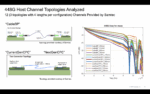
It lays the foundation for the Stochastics Resolution Gap
Chris Mack, the CTO of Fractilia, recently wrote of the “Stochastics Resolution Gap,” which is effectively limiting the manufacturability of EUV despite its ability to reach resolution limits approaching 10 nm in the lab [1,2]. As researchers have inevitably found, the shrinking dimensions of features targeted by EUV lithography have led to increasing stochastic variability operating at the molecular level [1,3,4]. This, in turn, leads to variations of feature width, feature position, edge roughness, and worst of all, yield-killing defects.
An SPIE paper by IMEC last year gave an updated yield model which strove to take into account the stochastic behavior of EUV lithography [5]. The model made use of defect density from calibrated wafer data and was said to be benchmarked against industry [5,6]. The model is essentially:
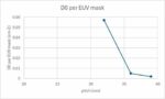
where systematic yield is an estimated value (98%) and random yield is given by the Poission model exp(-A*D0), with A being the die area (here taken to be 1 cm2), and D0 being the defect density. Since some layers require more than one mask, D0 would be the product of the defect densities per mask use. Since EUV stochastic effects get worse with smaller pitch, the corresponding D0 per use of EUV mask increases with pitch. In fact, there is a cliff that starts just below 40 nm pitch (Figure 1).
Figure 1. Defect density per EUV mask use from calibrated wafer data, owing to stochastic behavior [5].
Advanced nodes also use immersion ArF lithography (193i). In IMEC’s model, the defect density per 193i mask use is held fixed at 0.005/cm2 [5,6]. Table 1 gives the assumed D0 values per mask use for the 7nm and 5nm nodes.
Table 1. Defect density (per cm2) per mask use for 7nm and 5nm process nodes [5].
Note that there are several versions of 5nm nodes. N5M applies both 193i and EUV for metal patterning (one mask each), while N5 EUV applies EUV only (single exposure patterning) and N5C EUV adds an EUV cut mask for metal patterning. Likewise, for 7nm, N7C EUV is N7 EUV with an EUV cut mask added for metal patterning. N5M EUV has better D0 per mask due to a more relaxed M1 pitch (equal to gate pitch), while N5 EUV and N5C EUV used tighter M1 pitch, effectively a shrink compared to N5 193i and N5M.
Table 2. Number of 193i and EUV masks used per 7nm and 5nm layer, assumed in [5].
Assuming a 1 cm2 die area, the yields are calculated for each of the five layers (M1, V1, M2, V2, M3), according to the number of masks used, then the layer yields are multiplied together, and finally the systematic yield is multiplied by the result to give the total yield. For 7nm, we see in Figure 2 that although the use of fewer masks with EUV increases the yield, the difference from the all 193i case is small. For 7nm, 193i LELE (self-aligned) patterning is largely sufficient and actually cheaper than single exposure EUV [7,8].
Figure 2. Estimated yields for 7nm (all 193i/all EUV single exposure/all EUV, including cuts).
On the other hand, for 5nm, more layers are at tighter pitches, increasing the stochastic defect density from EUV. Thus, increasing EUV use actually increased the overall defect density, lowering yield (Figure 3).
Figure 3. Estimated yields for 5nm (all 193i/mixed 193i/EUV/all EUV single exposure/all EUV, including cuts).
The reason for the drastic change in trend is the much higher EUV defect density (0.057/cm2) at the tighter metal pitch. In fact, compared to the 193i defect density (0.005/cm2), it is 11 times higher, meaning its impact on yield would be the same as using eleven 193i masks in multipatterning!
Thus, IMEC’s updated yield model is the basis for the Stochastics Resolution Gap, as it can be projected that yield impact from stochastics outweighs intrinsic resolution in process choices for advanced nodes. Further tuning of the model would be beneficial, such as accounting for performance impact from roughness and edge placement error as well as CD variations. This spotlights the need for improved, high-volume metrology techniques for detecting these issues from EUV stochastics, definitely something that Fractilia would be happy to deal with.
References
[1] C. Mack, Stochastics: Yield-Killing Gap No One Wants to Talk About.
[2] J. Y. Choi et al., Proc. SPIE 13424, 134240A (2025).
[3] H. Fukuda, J. Appl. Phys. 137, 204902 (2025), and references therein; https://doi.org/10.1063/5.0254984.
[4] F. Chen, Facing the Quantum Nature of EUV Lithography.
[5] Y-P. Tsai et al., Proc. SPIE 12954, 1295404 (2024).
[6] Y-P. Tsai et al., Proc. SPIE 12052, 1205203 (2022).
[7] E. Vidal-Russell, J. Micro/Nanopatterning, Materials, and Metrology 23, 041504 (2024).
[8] L-Å Ragnarsson et al., EDTM 2022.
This article first appeared on Substack: IMEC’s Advanced Node Yield Model Now Addresses EUV Stochastics
Also Read:
Edge Roughness Differences Among EUV Resists
Facing the Quantum Nature of EUV Lithography
High-NA Hard Sell: EUV Multi-patterning Practices Revealed, Depth of Focus Not Mentioned