webinar banner AI 2026 v2

Cerebras AI Inference Wins Demo of the Year Award at TSMC North America Technology Symposium

Cerebras AI Inference Wins Demo of the Year Award at TSMC North America Technology Symposium
by Daniel Nenni on 12-07-2025 at 2:00 pm

Cerebras TSMC OIP 2025

This is a clear reminder of how important the semiconductor ecosystem is and how closely TSMC works with customers. The TSMC Symposium started 30 years ago and I have been a part of it ever since.  This event is attended by TSMC’s top customers and partners and is the #1 semiconductor networking event of the year, absolutely.

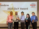
Cerebras Systems, the pioneer in wafer-scale AI acceleration, today announced that its live demonstration of the CS-3 AI inference system received the prestigious Demo of the Year award at the 2025 TSMC North America Technology Symposium in Santa Clara.

The winning demonstration showcased the Cerebras CS-3, powered by the industry’s largest chip, the 4-trillion-transistor Wafer-Scale Engine 3 (WSE-3), delivering real-time, multi-modal inference on Meta’s Llama 3.1 405B model at over 1,800 tokens per second for a single user, and sustaining over 1,000 tokens per second even under heavy concurrent multi-user workloads. Running entirely in memory with no external DRAM bottlenecks, the CS-3 processed complex reasoning, vision-language, and long-context tasks with sub-200-millisecond latency performance previously considered impossible at this scale.

TSMC’s selection committee, composed of senior executives and technical fellows, cited three decisive factors:
  1. Unprecedented single-chip performance on frontier models without multi-node scaling
  2. True real-time interactivity on models larger than 400 billion parameters
  3. Seamless integration of TSMC’s most advanced 5 nm technology with Cerebras’ revolutionary wafer-scale architecture

During the live demo, the CS-3 simultaneously served dozens of concurrent users running Llama 3.1 405B with 128k context windows, answering sophisticated multi-turn questions, generating images from text prompts via integration with Flux.1, and performing real-time document analysis—all while maintaining conversational latency indistinguishable from smaller cloud-based models.

“Wafer-scale computing was considered impossible for fifty years, and together with TSMC we proved it could be done,” said Dhiraj Mallick, COO, Cerebras Systems. “Since that initial milestone, we’ve built an entire technology platform to run today’s most important AI workloads more than 20x faster than GPUs, transforming a semiconductor breakthrough into a product breakthrough used around the world.”

“At TSMC, we support all our customers of all sizes—from pioneering startups to established industry leaders—with industry-leading semiconductor manufacturing technologies and capacities, helping turn their transformative idea into realities,” said Lucas Tsai, Vice President of Business Management, TSMC North America. “We are glad to work with industry innovators likes Cerebras to enable their semiconductor success and drive advancements in AI.”

The CS-3’s memory fabric provides 21 petabytes per second of bandwidth and 44 gigabytes of on-chip SRAM—equivalent to the memory of over 3,000 GPUs—enabling entire 405B-parameter models to reside on a single processor. This eliminates the inter-GPU communication overhead that plagues traditional GPU clusters, resulting in dramatically lower latency and up to 20x higher throughput per dollar on large-model inference.

The recognition comes as enterprises increasingly demand cost-effective, low-latency access to frontier-scale models. Independent benchmarks published last month by Artificial Analysis confirmed the CS-3 as the fastest single-accelerator system for Llama 3.1 70B and 405B inference, outperforming NVIDIA H100 and Blackwell GPU clusters on both tokens-per-second and time-to-first-token metrics.

TSMC’s annual symposium attracts thousands of engineers and executives from across the semiconductor ecosystem. The Demo of the Year award has previously gone to groundbreaking advancements in 3 nm and 2 nm process technology; this year marks the first time an AI systems company has claimed the honor.

Cerebras is now shipping CS-3 systems to customers in healthcare, finance, government, and scientific research. The company also announced general availability of Cerebras Inference Cloud, offering developers instant API access to Llama 3.1 405B at speeds up to 1,800 tokens/second—the fastest publicly available inference for models of this scale.

Bottom line: With this award from TSMC, Cerebras solidifies its position as the performance leader in generative AI inference, proving that wafer-scale computing has moved from bold vision to deployed reality.

Also Read:

TSMC Kumamoto: Pioneering Japan’s Semiconductor Revival

AI-Driven DRC Productivity Optimization: Revolutionizing Semiconductor Design

Exploring TSMC’s OIP Ecosystem Benefits

Breaking the Thermal Wall: TSMC Demonstrates Direct-to-Silicon Liquid Cooling on CoWoS®


CEO Interview with Pere Llimós Muntal of Skycore Semiconductors

CEO Interview with Pere Llimós Muntal of Skycore Semiconductors
by Daniel Nenni on 12-05-2025 at 12:00 pm

pere headshot alternative

Pere Llimós Muntal is the CEO and co-founder of Skycore Semiconductors, driving the strategy, business development, and growth of the company as it delivers next-generation power integrated circuit (IC) solutions for applications with extreme power density, efficiency, and form factor demands, such as data center power delivery.

Pere received the combined B.Sc. and M.Sc. degree in industrial engineering from the Polytechnic University of Catalonia in 2012, and a Ph.D. in Electrical Engineering from the Technical University of Denmark (DTU) in 2016, where he developed high-voltage and analog front-end ICs for portable ultrasound systems. He continued his research at DTU as a postdoctoral researcher and assistant professor, focusing on high-voltage integrated switched-capacitor power conversion.

His technical expertise includes switched-capacitor power conversion, high-voltage integrated circuit design, analog front-ends for ultrasonic transducers, and continuous-time sigma-delta A/D converters.

Today, he leads Skycore’s efforts to deliver advanced power IC solutions for next-generation data center HVDC architectures.

Tell us about your company?

Skycore Semiconductors is a Denmark-based fabless semiconductor company developing advanced Power Integrated Circuits (ICs) solutions for applications with extreme power density and efficiency demands, such as the 800V HVDC power architectures of the next generation AI data centers.

Our Power IC technology platform delivers extreme power density and efficiency in compact, flat form factors. This allows system designers to rethink how power is distributed in high-performance compute environments, especially as the industry moves from traditional 54 VDC systems to 800V HVDC architectures.

With roughly €7.5M raised to date, including our recent €5M seed round, we are scaling our team, deepening our partnerships, and preparing our first commercial products for market entry.

What problems are you solving?

AI data centers are hitting a physical limit when it comes to power. Today’s 54 VDC distribution cannot keep up with racks pushing beyond 200 kW. The current in the busbars, power density requirements, thermal constraints, and size limitations have become real bottlenecks.

Scaling today’s AI compute infrastructure requires a fundamental change in how data centers are powered, and 800V HVDC power architectures are the first step on that path.

Our technology enables the transition to 800V HVDC architectures, an industry shift that is now accelerating across hyperscalers and accelerated compute vendors. Our Power IC solutions unlock new architecture possibilities which are the key to scaling the compute and power density for the next generation of AI factories.

What application areas are your strongest?

Our strongest application area is AI compute infrastructure, more specifically the power delivery path inside high-density, high-efficiency data centers moving to HVDC architectures.

That said, the underlying technology platform provides benefits for any application with extreme power demands, such as high-performance computing, EVs and advanced robotics. But our immediate focus is clear: enabling the rapidly growing ecosystem of 800V AI data centers.

What keeps your customers up at night?

Their main question is how to continue to scale compute without running into the limits of physics.

They are facing exponentially growing power demands, insufficient rack-level power density, rising thermal challenges, and pressure to deliver more performance per watt, while maintaining reliability and compute scalability.

The shift to 800V HVDC is happening because customers know the current approach cannot scale. The question is not whether the transition is coming, but how fast can they get there, and with what technology. We provide them with the technology to cross that gap.

What does the competitive landscape look like and how do you differentiate?

The competitive landscape is a mix of traditional power semiconductor players and newer efforts focused on dense power conversion. But most existing solutions were never designed for the demands of HVDC power delivery in AI data centers. They are adaptations of legacy solutions.

We design our solutions from the ground up to be inherently scalable and meet the evolving demands of HVDC power architectures. We aim to provide the building blocks for the power architectures that AI infrastructure will rely on for the next decade.

Our differentiation is centered around three pillars:

  1. Power IC technology platform
    Silicon-proven and tailored for applications with extreme power demands and fast development cycles.
  2. Scalable power solutions
    Our power solutions are modular and scale in power, voltage and conversion ratio to meet the growing demands of power, efficiency, and trend towards higher-voltage architectures.
  3. Architecture alignment with the development of next-generation AI data centers
    Alignment via industry partnerships, strategic providers, and development projects as members of the Open Compute Project (OCP) and Berkeley Power & Energy Center (BPEC), alongside prominent industry members like Nvidia, Google, Intel, Tesla, and Analog Devices.
How do customers normally engage with your company?

Our typical engagement model is collaborative. We work closely with hyperscalers, system vendors, and power architecture teams who are planning or already deploying the transition to HVDC.

This often begins with technical exploration and architecture definition, followed by co-development projects to tailor our Power IC solutions to their system-level requirements.

Because we operate at the intersection of semiconductor technology and data center system design, early engagement allows customers to shape the integration of our ICs into their next-generation racks and compute platforms. Our goal is to be a long-term partner and enabler, not just a component provider.

Also Read:

CEO Interview with Brandon Lucia of Efficient Computer

CEO Interview with Dr. Peng Zou of PowerLattice

CEO Interview with Roy Barnes of TPC


Podcast EP321: An Overview of Soitec’s Worldwide Leadership in Engineered Substrates with Steve Babureck

Podcast EP321: An Overview of Soitec’s Worldwide Leadership in Engineered Substrates with Steve Babureck
by Daniel Nenni on 12-05-2025 at 10:00 am

Daniel is joined by Steve Babureck, executive vice president of strategy and president of Soitec USA. He joined the company in 2011 and held various positions including head of the finance department of the solar business in the United States, head of strategic marketing, and head of Group investor Relations in San Diego and Singapore.

Steve shares some of his motivation with Dan regarding taking on the role of president of Soitec USA. He describes the worldwide footprint Soitec has developed to deliver engineered substrates to a wide range of customers and applications. He explains how the company works with fabs, fabless organizations, system integrators and end customers across many applications that includes low power AMS, edge processing, silicon photonics, and RF for many markets including AI, automotive and data centers.

Steve explains that developing closer relationships with system integrators, fabless companies and end customers in the US will help to expand Soitec’s worldwide footprint and increase the company’s leadership in the development and deployment of many forms of engineered substrates.

See SOITEC at IEDM.

The views, thoughts, and opinions expressed in these podcasts belong solely to the speaker, and not to the speaker’s employer, organization, committee or any other group or individual.


ClockEdge Delivers Precision, Visibility and Control for Advanced Node Clock Networks

ClockEdge Delivers Precision, Visibility and Control for Advanced Node Clock Networks
by Mike Gianfagna on 12-05-2025 at 6:00 am

ClockEdge Delivers Precision, Visibility and Control for Advanced Node Clock Networks

At advanced nodes, the clock is no longer just another signal. It is the most critical and sensitive electrical network on the chip, and the difference between meeting performance targets and missing the tape-out often comes down to a few picoseconds, buried deep inside the clock distribution network. Yet many design teams still rely on verification methods built for a world where margin was abundant and physics was forgiving. That world no longer exists.

ClockEdge delivers the SPICE-level precision, visibility and control that advanced node clock networks now require.  Let’s examine how the company meets advanced node challenges and opens new innovation opportunities.

What ClockEdge Delivers and Why

At 28 nm, wide guard bands and coarse approximations could cover up hidden clock behavior — at a full design cost under $50M. At 3 nm and 2 nm, margins have collapsed, variability dominates, and a single tape-out can exceed $700M. With stakes this high, any inaccuracy in clock analysis becomes an unacceptable risk.

Modern clock networks run so close to physical limits that even small inaccuracies in timing, jitter, power, or aging analysis can trigger cascading failures in silicon. These interactions are invisible to traditional flows; designs may appear to close timing, and meet power and reliability targets, yet still fail in in silicon. The problem is a lack of accuracy, visibility and control of the all-important clock network. The traditional approach is to use static timing analysis and SPICE for critical paths only, due to the capacity and runtime limitations of SPICE.

This approach misses subtle but critical interactions that cause the previously mentioned cascading failures.

ClockEdge tames this problem with a family of SPICE-accurate analysis engines for timing, power, jitter, and aging analysis of clock circuits. A patented SPICE-accurate digital simulation engine delivers full SPICE precision without the capacity and speed limitations that make traditional SPICE impractical for full-clock analysis.

ClockEdge’s Veridian Suite delivers sign-off precision at real-world scale and speed, applying SPICE-accurate truth across the entire clock network. It uncovers interactions that conventional flows miss and exposes how nanometer effects directly shape clock performance and reliability.

Components of the Veridian suite include:
  • vTiming: Delivers SPICE-accurate, full-clock visibility from PLL to flop, exposing rail-to-rail failures, duty-cycle distortion, and hidden timing risks that define silicon performance.
  • vPower: Pinpoints and reduces clock tree power using SPICE-accurate, power-aware analysis, enabling targeted optimization and fast, iterative design refinement.
  • vAging: Models NBTI, HCI, and other stress effects to predict how clock paths degrade over time, exposing aging-induced timing drift, duty-cycle distortion and reliability loss.
  • vJitter: Analyzes power supply induced noise with SPICE-level precision, revealing sub-picosecond timing variation and clock instability long before silicon.

Completing the picture is vHelm, the designer’s command center. vHelm provides instant visibility into how every clock decision affects timing, power, jitter, and aging, all at once.

Clock design is a system of tight interdependencies, where a single change that improves timing can degrade power, jitter, or aging unless these effects are evaluated together. vHelm exposes these interactions so designers can explore what-if scenarios, apply virtual ECO adjustments, and see waveform-accurate results in real time.

vHelm provides a unified workspace where designers can perform tasks such as resize a buffer, adjust a constraint, change a gating strategy, or test a topology change and see how the entire clock network responds. Timing margins, power consumption, edge quality, and long-term reliability are all updated side by side, making design trade-offs clear before decisions are committed.

Together, the Veridian suite and vHelm deliver the breakthrough accuracy, visibility and control that advanced node clock networks can no longer function without. Thanks to ClockEdge, optimized clocking is now within reach for all design teams. There are many benefits. Some are illustrated in the graphic below.

Key Benefits Delivered by ClockEdge

To Learn More

I’ve just scratched the surface on what ClockEdge has to offer and how it will impact the quality and robustness of your next design. If qualities such as better design performance and longer device lifetimes appeal to you, check out ClockEdge here.  If you’d like to see how the tool can help you in more detail you can reach out to set up a discussion here.  And that’s how ClockEdge delivers precision, visibility and control that advanced node clock networks now demand.  


CEO Interview with Haber Ma of ADCERAX

CEO Interview with Haber Ma of ADCERAX
by Daniel Nenni on 12-04-2025 at 12:00 pm

Haber Ma ADCERAX

Haber Ma is the CEO of ADCERAX and leads the company’s global strategy in advanced ceramic materials for semiconductor and high-performance industrial applications. With a background in engineering, precision manufacturing, and international supply chain development, he has overseen ADCERAX’s transition from a traditional ceramics producer to a specialized supplier of semiconductor-grade alumina, zirconia, SiC, and Si₃N₄ components.

Haber has played a key role in establishing ADCERAX’s material engineering capabilities, machining precision standards, and customer collaboration model focused on reliability, purity, and long-term stability. Under his leadership, the company has expanded its portfolio to include ceramic robot arms, ESC-related components, plasma-erosion-resistant ceramics, and advanced furnace materials. He advocates for deeper integration between ceramic material science and semiconductor equipment engineering to support the industry’s scaling and purity demands.

Tell us about your company.

ADCERAX is an advanced ceramics manufacturer specializing in semiconductor-grade alumina, zirconia, silicon carbide (SiC), silicon nitride (Si₃N₄), aluminum nitride (AlN), and ZTA materials. Our mission is to deliver high-purity, high-reliability ceramic components that support the performance, stability, and cleanliness requirements of modern semiconductor equipment.

We focus heavily on engineering collaboration with tool OEMs and subsystem suppliers, providing fully custom mechanical parts, chamber insulation ceramics, ceramic end effectors, electrostatic-chuck-related components, and structural parts for vacuum, etch, deposition, and thermal processing systems. With vertically integrated machining, precision grinding, and testing capabilities, ADCERAX helps customers accelerate development, improve system reliability, and achieve long-term supply chain resilience.

What problems are you solving?

Semiconductor manufacturing environments push materials to extremes—high plasma energy, aggressive chemistries, rapid thermal cycling, and strict particle control. Many traditional materials cannot maintain dimensional stability, surface integrity, or dielectric reliability under these conditions. The smallest contamination event or micro-crack can jeopardize yield.

ADCERAX addresses these challenges with engineered ceramics that maintain high mechanical strength, low particle generation, and exceptional corrosion resistance. Our SiC and Si₃N₄ components withstand plasma erosion in etch and CVD chambers, while high-purity alumina and AlN ensure dielectric stability for wafer handling and isolation applications. In thermal processing, components such as precision alumina tube solutions support consistent temperature distribution and long-term furnace reliability. Our goal is to remove material-related failure modes so customers can focus on equipment performance rather than replacement cycles.

What application areas are your strongest?

Our strongest applications lie in semiconductor equipment—particularly where extreme environments demand stable, clean, and long-lasting ceramic components. Key product categories include:

  • Electrostatic chuck (ESC) ceramics: high-purity dielectric materials and structural components for vacuum and plasma environments.
  • Ceramic robot arms and end effectors: ultra-clean, lightweight, and thermally stable components for wafer transport and automation.
  • LPCVD / diffusion furnace tubes: alumina and quartz-alternative ceramics for long-cycle thermal processing.
  • Chamber insulation and isolation ceramics: rings, plates, and liners engineered for plasma-erosion resistance.
  • SiC and Si₃N₄ mechanical components: ideal for corrosive chemistries and high-temperature subsystems.

These applications leverage our expertise in purity control, microstructure engineering, and precision machining for semiconductor equipment platforms.

What keeps your customers up at night?

Semiconductor equipment manufacturers face growing challenges around reliability, contamination control, and supply chain stability. A single ceramic component failure—whether from plasma erosion, thermal shock, or insufficient machining precision—can lead to extended downtime or yield loss.

Customers worry about:

  • particle generation from material microfractures
  • long-term erosion in aggressive plasma chemistries
  • surface roughness drift affecting chamber cleanliness
  • CTE mismatch causing assembly instability
  • inconsistent global supply of critical ceramic parts

At ADCERAX, we help mitigate these risks through rigorous material qualification, tight-tolerance machining, and repeatable production processes. Our engineering collaboration model ensures each component is optimized for the customer’s system environment rather than treated as a generic ceramic part.

What does the competitive landscape look like and how do you differentiate?

The market for semiconductor ceramics is highly specialized, with a small group of manufacturers offering semi-grade purity and machining accuracy. Many suppliers focus on standard industrial ceramics, but semiconductor applications require an entirely different level of microstructural control, polishing precision, and contamination management.

ADCERAX differentiates by combining:
  • semi-grade purity control for low alkali and low metallic contamination
  • tight-tolerance machining for high-precision wafer handling and chamber components
  • advanced materials portfolio (Al₂O₃, AlN, SiC, Si₃N₄, ZTA) aligned with semiconductor needs
  • custom component engineering rather than fixed catalog items
  • fast prototype-to-production cycles, enabling faster OEM development timelines

Our integration of engineering, machining, and materials expertise allows us to serve as both a supplier and a technical partner.

What new features or technology are you working on?

ADCERAX is expanding its R&D around high-purity ceramics for next-generation etch and deposition platforms. This includes improvements in:

plasma-erosion-resistant SiC and Si₃N₄ for advanced etch chemistries
high-thermal-uniformity alumina structures for diffusion and LPCVD systems
ultra-flat, ultra-clean ceramic plates for wafer handling subsystems
advanced polishing and surface engineering to reduce particle generation

We are also developing enhanced metrology and inspection methods to support OEM qualification requirements, including micro-defect detection and advanced surface analysis. Our long-term direction is enabling ceramic components that last longer, shed fewer particles, and support higher equipment uptime.

How do customers normally engage with your company?

Most customers approach ADCERAX through engineering-driven collaboration. They typically provide drawings, CAD files, or prototype requirements, and our team works closely with their engineers to refine material selection, tolerances, and design features.

We support the full cycle from prototype builds to mass production, offering:
  • material and design consultation
  • rapid sampling and custom machining
  • batch production with strict quality control
  • global logistics support for long-term supply programs

For semiconductor OEMs and subsystem suppliers, we often join early in the design phase to ensure every ceramic part meets performance, reliability, and cleanliness expectations. Website: https://www.adcerax.com

Also Read:

CEO Interview with Pere Llimós Muntal of Skycore Semiconductors

CEO Interview with Brandon Lucia of Efficient Computer

CEO Interview with Dr. Peng Zou of PowerLattice


WEBINAR: Defacto’s SoC Compiler AI: Democratizing SoC Design with Human Language

WEBINAR: Defacto’s SoC Compiler AI: Democratizing SoC Design with Human Language
by Daniel Nenni on 12-04-2025 at 10:00 am

webinar square2025 (1)

Modern chip design has reached unprecedented levels of complexity. Today’s System-on-Chip (SoC) designs integrate multiple processors, complex memory hierarchies, sophisticated interconnects, and much more. All requiring orchestration using complex EDA tool flows. Months are routinely lost to configuration errors, tool-chain mismatches, and manual stitching of subsystems

While these tools are powerful, they demand deep expertise not just in chip architecture, but in the tools themselves. Design teams spend numerous hours navigating complex interfaces, scripting configurations, and troubleshooting tool-specific syntax. The learning curve is time consuming, the margin for error is high, and the time-to-market pressure continuously.

The emergence of artificial intelligence is fundamentally changing how we get access to the information and use complex tools. What was requiring specialized training and years of experience can now be accessed through natural language conversation. But can this transformation extend to something as complex as chip design?

REGISTER NOW

What if you could skip most of that and simply describe—in plain English—what you need?

Defacto Technologies believes the answer is now “yes.” Their new SoC Compiler AI Assistant turns natural-language conversations into complete, synthesis-ready SoC designs in a fraction of the usual time.

The Defacto AI assistant interoperates seamlessly with both commercial and open source LLMs to leverage natural language queries and help building pre-synthesis complex SoC designs with a significant decrease in design cycles. This AI assistant is open for non-design experts to generate complex pre-assembled subsystems and top level SoCs ready for implementation and verification.

Because the assistant sits on top of Defacto’s production-grade integration engine (already used by tier-1 semiconductor companies), the output isn’t a rough prototype or “AI hallucination”. It’s the same quality you would get from a senior integration team.

This dramatically lowers the expertise barrier. Architects can explore trade-offs without waiting for integration engineers. Junior designers become productive in few days. Entirely new players, startups, even systems companies that previously outsourced chip design, can now create custom silicon in-house.

Join Defacto’s upcoming webinar on Tuesday, December 9, 2025 at 10:00 AM PST and see it for yourself.

This isn’t just theory or slides, you’ll see how:
  • Building an SoC using conversational natural language
  • Real-time design optimizations through simple dialogue
  • Integrating Defacto’s SoC Compiler AI into internal development environments

CEO & CTO Chouki Aktouf will explain the architecture and vision, while R&D engineer Hugo Brisset performs a live, no-slides, no-safety-net demonstration: building a production-grade SoC from a blank project using only voice and natural language, integrating it into a standard EDA environment, and performing on-the-fly optimizations, all in real time.

Attendees will leave understanding:
  • How natural language actually drives industrial-strength EDA tools today
  • Measured productivity gains and remaining limitations
  • What infrastructure you need to deploy this in your own flows

If you’re a chip architect wondering whether AI is still hype, an engineering manager fighting tape-out schedules, or a technical decision-maker evaluating next-generation design platforms, this is the session that will shift your perspective.

Seats are limited. Register now and witness the moment SoC integration becomes as simple as having a conversation.

Also Read:

Defacto at the 2025 Design Automation Conference #62DAC

SoC Front-end Build and Assembly

Video EP8: How Defacto Technologies Helps Customers Build Complex SoC Designs


An Assistant to Ease Your Transition to PSS

An Assistant to Ease Your Transition to PSS
by Bernard Murphy on 12-04-2025 at 6:00 am

PSS Assistant min

At times it has seemed like any development in EDA had to build a GenAI app that would catch the attention of Wall Street. Now I see more attention to GenAI being used for less glamorous but eminently more practical advances. This recent white paper from Siemens on how to help verification engineers get up to speed faster with PSS is a good example of a trend that uses GenAI to enhance engineering productivity in complex flows, rather than upending flows. While revolutionary new methods may continue to excite, these more modest advances will pay off in the short term and may ultimately be more durable.

Verification intent and the tension between PSS and UVM

A powerful way to enhance productivity is to work directly with high-level intent, in this case verification test descriptions, rather than implementation, assuming you have a way to generate the implementation from that intent. UVM is the default representation for test intent today, but its intent is entangled with UVM implementation details.

PSS on the other hand is very good at representing high-level intent, rather than implementation, and can directly generate UVM and C testbenches to drive standard DV flows. But PSS is less familiar to DV engineers who have already invested in learning their way around UVM features and dialects and have little time to learn new approaches.

Does the methodology even need to change? Unfortunately designs continue to get more complex, and DV engineers must continue to move with the times, just like everyone else. But it’s not unreasonable for them to expect help in making that transition. This is where Questa One’s Portable Stimulus Assist becomes useful, guiding PSS novices to build their own PSS models through natural language prompts.

Why not use GenAI to assist UVM generation?

Good question. A GenAI assistant could cut out a PSS middleman and go straight to generating UVM. However, the author of the whitepaper has a detailed answer for why this is not the best approach, which reinforces a suspicion I have about most effective uses of GenAI technology: that GenAI models often perform best when the expression gap between the initial request/prompt and deliverable is not too wide.

I see this also in spec refinement tools and in modern prompt guidance tools. When the output is still reasonably close to intent, it is easier for us to spot and correct mistakes. But if the tool must cross a wider gap, going straight to implementation, it is harder for us to spot where it may have gone wrong, especially for subtle mistakes.

A related problem is that crossing wider gaps with confidence depends on more extensive training corpora. There are many possible ways to implement a piece of intent. Few of these would probably meet best design practices, but without guided fine-tuning in training there is no reason to expect those best practices will necessarily be honored.

In contrast, developing a PSS model starting from a prompt should be much simpler since it will be easier for a DV engineer to check and refine intent in the PSS model against expectations. And once captured and approved in PSS, translation to a UVM or other model is pushbutton, because that deterministic (non-AI) capability is already built into PSS tools and libraries.

The white paper elaborates specific examples of why a direct GenAI to UVM generation would be challenging.

Nice paper and a very practical application. The link to the paper is HERE.


Accelerating NPI with Deep Data: From First Silicon to Volume

Accelerating NPI with Deep Data: From First Silicon to Volume
by Kalar Rajendiran on 12-03-2025 at 10:00 am

proteanTecs Multi Pillar Technology

For decades, semiconductor teams have relied on traditional methods such as corner-based analysis, surrogate monitors, and population-level statistical screening for post-silicon validation. These methods served well when variability was modest, and timing paths behaved predictably. However, today’s advanced nodes and complex architectures expose the limitations of these approaches. Local process variation, workload-driven activation, dynamic voltage droop, aging, and subtle defects create path-specific outcomes that traditional monitors cannot capture. Proxy monitors cannot reflect real functional paths under real operating conditions, leaving engineers blind to critical performance, quality, and reliability issues.

As competition and time-to-market pressures increase, teams cannot afford the iterative cycles required to reconcile design assumptions with actual silicon behavior.

proteanTecs recently hosted a webinar addressing this very topic and presented its solution for accelerating New Product Introduction (NPI). proteanTecs’ Alex Burlak, Executive Vice President, Test and Analytics and Noam Brousard, Vice President, Solutions Engineering led the webinar session. The webinar titled “Accelerating NPI with Deep Data: From First Silicon to Volume” presented a new approach that replaces assumptions with real-time, on-chip insight, enabling teams to detect issues early, characterize power/performance confidently, accelerate debug, and optimize qualification.

The Need for Deep Visibility Across the NPI Lifecycle

Modern NPI requires visibility into every chip, in every scenario. Engineers need to understand where individual devices might fail, how variability affects functional paths, and how workload, voltage, and temperature interact to create real operational limits. Traditional methods cannot provide this insight, leaving teams reactive and slow to identify critical issues. This webinar demonstrated that high-resolution, chip-specific data allows teams to characterize actual performance, detect early parametric drift, and unify insights across design, test, and validation phases.

On-Chip Monitoring with Advanced Design-Aware Analytics

proteanTecs provide a HW IP Monitoring system that includes monitoring agents and an infrastructure that provides the control framework. The on-chip agents are embedded, ultra-lightweight on-chip monitors engineered to extract “deep data” – including design profiling, material classification, performance degradation, workload impact, and operational effects. Rather than monitoring only high-level counters or traditional test structures, these agents sit close to the actual circuitry, collecting granular telemetry throughout the chip’s entire operational life.

By capturing this deep data from within the device and applying advanced machine learning, these agents enable early detection of reliability risks, performance drift, power inefficiencies, and system degradations, long before they become visible at the system level.

Timing Margin Monitoring: Real-Time Insight from Real Functional Paths

proteanTecs Margin Agents deliver this visibility by embedding lightweight monitors directly into real timing paths. These agents measure instantaneous slack and are sensitive to operational conditions, process variations, aging, and latent defects. Unlike proxy circuits, they capture the real limits of a chip, providing precise insight into performance and reliability boundaries.

Alex Burlak opened the webinar with a use case demonstrating how proteanTecs enables customers to correlate simulation expectations with real silicon behavior.

By aggregating agent data from multiple test stages including wafer sort, final test, and system-level evaluation into a centralized analysis environment, engineers can directly align design intent with silicon results.

By examining process signatures captured by Profiling Agents across standard cells, teams can quantify process variation relative to design corners and link it to metrics such as Fmax, VDDmin, and the impact on yield. This insight supports detailed root-cause analysis, helping engineers identify why certain chips run faster or slower and isolate variation sources, such as clock-path versus data-path effects or on-chip variation (OCV).

To accelerate characterization, proteanTecs offers a Smart Material Selection algorithm. After initial test data collection, this algorithm identifies the most representative subset of chips (e.g., 50 out of 1,000) that best captures process variability. By focusing on these representative devices, characterization efforts, such as voltage, temperature, or workload sweeps, become far more efficient and comprehensive. Advanced HTOL Methodologies for Device Qualification.

Next, Alex presented a use case on High-Temperature Operating Life (HTOL) testing. Using proteanTecs’ Profiling and Margin Agents, customers can track degradation over time, collecting data at intervals such as 0, 48, 500, and 1,000 hours. This enables quantification of parametric drift and more accurate decisions about guard-banding and reliability.

Unifying Data from Design, Test, Validation, and Characterization

proteanTecs’ agents produce consistent, high-resolution data throughout the NPI lifecycle. Engineers can trace performance trends from wafer sort through ATPG, functional testing, HTOL, qualification, and high-volume production. They can even continue monitoring in the field. This unified dataset allows teams to detect deviations early, correlate results across test stages, and communicate insights efficiently between design and product engineering teams. By grounding decisions in actionable data rather than assumptions, organizations reduce risk and accelerate time-to-market.

Smart Models: Eliminating Yield–Quality Trade-Offs

The webinar highlighted smart models that leverage agent data to resolve the traditional trade-off between yield and quality. Instead of relying on global statistical thresholds, smart models analyze each chip against its expected electrical behavior. They identify true outliers based on high-resolution, chip-specific measurements, avoiding the need to discard potentially good devices or compromise quality. Noam emphasized that this approach allows teams to maintain high yield without sacrificing reliability, effectively providing both efficiency and assurance across production.

Continuous Monitoring during HTOL and In-Field Monitoring

The solution also supports continuous monitoring during HTOL and in-field operation. Engineers can observe degradation trends in real time, rather than waiting for post-stress readouts. Noam  demonstrated that this enables early detection of unexpected behavior, identification of hotspots, and rapid response to process or setup issues. In-field operation benefits similarly: Margin Agents operate without interrupting workloads, providing continuous visibility into aging, performance drift, and reliability over the product’s lifetime. By extending NPI insight into actual deployment, teams can react proactively, reducing risk and improving long-term product performance.

Summary

Alex and Noam demonstrated through live demos on case studies that deep on-chip data transforms NPI by providing real-time, high-resolution insight into each chip’s power, performance and reliability. On-chip agents reveal true performance limits, smart models identify outliers without compromising yield, and continuous monitoring provides actionable information from wafer sort through in-field operation.

By embedding deep data and analytics into the NPI workflow, semiconductor teams gain confidence, clarity, and control. Every chip becomes its own source of truth, and every stage of the NPI pipeline benefits from actionable insight. The result is faster ramp, higher quality, fewer surprises, and a fundamentally more predictable transition from first silicon to volume production.

To watch the on-demand webinar, click here: https://hubs.la/Q03W0k2V0

To learn more, visit:

proteanTecs/technology

proteanTecs/solutions

Also Read:

Failure Prevention with Real-Time Health Monitoring: A proteanTecs Innovation

Podcast EP313: How proteanTecs Optimizes Production Test

Thermal Sensing Headache Finally Over for 2nm and Beyond


We Need to Turn Specs into Oracles for Agentic Verification

We Need to Turn Specs into Oracles for Agentic Verification
by Bernard Murphy on 12-03-2025 at 6:00 am

Spec as an oracle min

The natural language understanding now possible in LLMs has raised interest in using specs as a direct reference for test generation, to eliminate need for intermediate and fallible human translation. Sadly, specs today are not an infallible source of truth for multiple reasons. I am grateful to Shelly Henry (CEO of MooresLab) for his insights into the realities of spec evolution in production settings. Shelly and his team have many years of design experience across several enterprises, most recently as alumni of the Microsoft Silicon Group.

Today’s spec as an oracle – you wish

Architecture specs go through a development cycle, as do all aspects of design and verification, and those specs are not perfect on first pass just as is the case for other deliverables in the design flow. An architect is responsible for building the specification, starting from customer requirements, considering what can be leveraged from other projects and what must be redesigned or upgraded to meet those new specs. The architect may be able to rely on a modeling group to do some virtual prototyping, testing for throughput, latencies, other metrics. Once they feel their rough model looks good they will start writing their spec. In what follows I’ll focus on the spec as guidance for hardware design verification though it equally should guide hardware and firmware design.

Working on the spec you need to start test planning will be the architect’s primary focus for a while, but not their only focus as they continue to manage other tasks already in their pipeline. Their first release may be a 0.5 version, covering perhaps 70% of what they considered up to this point. Again, a decent representation but not guaranteed to be perfect. Good enough to start design and verification schedule and resources.

Over time they will add to and refine the spec based on their own ideas, feedback from the customer and from you. Eventually the spec is frozen (Shelly suggests around halfway into the design schedule, though your mileage may differ). Within that window, between the 0.5 release and freeze, the spec is changing. There may be contradictions or missing information. There may also be ambiguities: the spec defines a feature but leaves too much open for you to be certain about expected behavior in all cases.

You email the architect for clarification. That turns into a thread, and you eventually agree on a resolution. But this outcome doesn’t always get back into the spec, or maybe it does but not fully reflecting the agreement you thought you had. Worse yet, you call the architect, agree on a resolution for which you make a note – somewhere. It’s easy to see how mistakes can happen despite good intentions all round. Unfortunately, there is no verification methodology to definitively prove that a spec fully reflects the expectations of all stakeholders. Perhaps disconnects will surface pre-silicon, perhaps not. Is this really the best that we can do?

How we could turn a spec into a robust oracle

Start with what we already can do. Input the 0.5 spec into an LLM-based agent and have that agent generate questions to the LLM to elaborate verification requirements based on know-how already captured in that LLM model. What are the standard types of tests that should be performed around a DDR interface in this class of designs for example?

There’s no need to digest a full spec in one gulp, likely impossible anyway given the bounded prompt windows that LLMs support. Specs are naturally organized by chapters and sections to respect the limited abilities of us fallible humans, much more amenable to LLM processing.

Agent questions shouldn’t ask how such tests should be performed – that is the concern of later test synthesis flows. Here we want to refine the test specification to add more descriptive detail around what behavior is expected. The detail the architect or you would have added to the spec if time and fallible memories allowed. Very likely this may involve timing diagrams, maybe FSM diagrams, block diagrams to elaborate clock and reset control, or how domain crossings are handled.

As the spec evolves, the agent should be able to digest mail threads, DM threads, notes, and use that information for further refinement. Ensuring a central source of truth, while also clarifying where changes originated and what they impacted, by revision. Making it much easier for stakeholders to review and mutually agree that this refined version fully reflects what they wanted.

Turning a spec into an oracle is an essential first step in an agentic verification flow. Filling in holes, correcting inconsistencies, resolving ambiguities and testing that the spec itself provides enough detail to drive comprehensive test generation. This seems to me to be a no-brainer. If you’re curious, you might want to talk to the folks at MooresLab.ai.


Accelerating SRAM Design Cycles: MediaTek’s Adoption of Siemens EDA’s Additive AI Technology at TSMC OIP 2025

Accelerating SRAM Design Cycles: MediaTek’s Adoption of Siemens EDA’s Additive AI Technology at TSMC OIP 2025
by Daniel Nenni on 12-02-2025 at 10:00 am

Siemens MediaTek TSMC OIP 2025

In the competitive vertical of mobile System-on-Chip development, SRAM plays a pivotal role, occupying nearly 40% of chip area and directly impacting yield and performance. The presentation “Accelerating SRAM Design Cycles With Additive AI Technology,” co-delivered by Mohamed Atoua of Siemens EDA and Deepesh Gujjar of MediaTek at TSMC’s Open Innovation Platform, addresses the verification challenges in advanced nodes like TSMC’s N2P process. As mobile SoCs push for lower minimum operating voltages (Vmin) to enhance power efficiency, device variations intensify, necessitating rigorous statistical yield qualification: 6-sigma for bitcells and 4-4.5 sigma for periphery logic. Traditional brute-force Monte Carlo simulations, while accurate, are computationally intensive and time-consuming, often leading to iterative design cycles that delay production.

The core motivation stems from these iterative workflows. Failures in verification prompt design fixes, PDK revisions, simulator updates, or additional PVT corners, each requiring full re-runs. MediaTek, leveraging Siemens EDA’s Solido tools, sought a more efficient approach. Enter Additive Learning technology, an AI-driven methodology integrated into the Solido Design Environment. This innovation retains and reuses AI models and simulation data from prior jobs, drastically reducing simulations in subsequent iterations without compromising SPICE-level accuracy.

Solido’s suite includes the High-Sigma Verifier and PVTMC Verifier, both enhanced by Additive Learning. HSV enables verifiable high-sigma analysis, achieving 6-sigma yield verification in thousands of simulations—up to 1,000-1,000,000,000x faster than brute force. PVTMC provides full-coverage verification across PVT corners plus Monte Carlo, 2-10x faster than traditional methods, excels at outlier detection. In traditional flows, five iterations might consume 50 hours; with Solido’s iterative workflow, this drops to 5 hours, saving days or weeks in chip schedules.

The Additive Learning Engine automatically detects reuse opportunities, drawing from a lightweight, optimized Reusable AI Datastore. This datastore supports multi-user access, parallel read/write, and small disk footprints, allowing deletion of full DE results while preserving speedup potential. It stores AI models and past data for fast lookups, ensuring seamless integration into workflows like design sizing changes or PDK updates.

MediaTek’s results demonstrate tangible benefits. In Case 1, verifying 5-sigma bitcell write margin on N2P (clock-to-bitcell flip), the base run required 2,500 simulations, yielding a mean of 120.1 ps and 5-sigma of 131.2 ps. Post-design fix (Vt changes in write driver and column mux), Additive Learning completed verification in just 29 simulations, a 67x speedup, with mean 121.8 ps and 5-sigma 132.5 ps. Case 2 involved 4-sigma instance-level verification (clock-to-data out), where the original 300 simulations gave mean 167.4 ps and 4-sigma 173.1 ps. After Vt updates in control/IO blocks, Additive Learning used 15 simulations (20x faster) matching full re-run results (mean 198 ps, 4-sigma 204.6-204.8 ps).

This technology’s broader adoption underscores its production-grade maturity. NVIDIA, for instance, employs Additive Learning in AI-powered standard cell verification, achieving speedups on incremental runs amid rising design complexity beyond 5nm. Siemens EDA highlights up to 100x boosts to existing AI techniques for verification efficiency. As nodes shrink, such tools are essential for maintaining accuracy while compressing cycles, enabling faster time-to-market for high-yield SoCs.

Bottom line: Additive Learning transforms SRAM design from a bottleneck into an agile process: fast, accurate, and automatic. By reusing models across iterations PDK revisions, sizing tweaks, or tool updates, it exemplifies AI’s role in EDA, as evidenced by MediaTek’s 20-67x gains. This collaboration between Siemens EDA and MediaTek not only accelerates mobile innovation but sets a benchmark for AI integration in semiconductor workflows, promising even greater efficiencies in future nodes.

Also Read:

Transforming Functional Verification through Intelligence

Why chip design needs industrial-grade EDA AI

Hierarchically defining bump and pin regions overcomes 3D IC complexity

CDC Verification for Safety-Critical Designs – What You Need to Know