Wednesday was the last day at #62DAC for me and I attended an Exhibitor Session entitled, Engineering the Semiconductor Digital Thread, which featured Vishal Moondhra, VP Solutions Engineering of Perforce IPLM and Michael Munsey, VP Semiconductor Industry at Siemens Digital Industries. Instead of just talking from slides, they did a back and forth discussion in rapid fire. Mike Gianfagna previously blogged about the strategic announcement between the two companies, unifying software and silicon across the ecosystem.
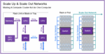
Siemens has been offering their digital twin methodology for several years now, and the two companies have worked together by integrating IPLM with IC tools. In the present era the trend is software defined products.
Michael – Just look at iOS on the iPhone with constant upgrades over time, and all of the apps are upgradable. Decisions were made up front, where SW was defined for new features to be constantly added. A smart phone can lock up accidentally and still be acceptable, but not so for a car, so safety is critical for some applications. We need verification plus a mapping back to requirements.
Vishal – Yes, we need high reliability in some fields with traceability., where we connect top level product marketing with requirements. There are Siemens tools for test and validation, then they are connected back into IP management.
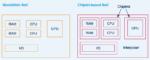
Micheal – For 3D IC data requirements, we see a mix and match of all EDA vendors files with meta data being used together.
Vishal – Using IP and chips and boards, mechanical systems, SW stacks, all tied together so that the system can be verified together in concert. Siemens and other vendors together can solve this, so we see that with SW defined products it demands collaboration.
Michael – In data centers they require infrastructure like chilled water, AC needs, cooling racks, all traced down to chips, boards and systems. How the design of past data centers may not be sufficient for future centers, because we need a way to analyze power profiles before silicon arrives.
Vishal – All tools need a common platform to exchange and manage metadata. All tools need to deposit and exchange data seamlessly, like in this new deal. We have design data, metadata, workflows, and a pool of info to train AI models now. On each block we know the version of tools that were run on it.
Michael – Siemens has invested in AI with Solido tools for ML to improve verification., then we announced a new EDA AI platform this week. We want to optimize both locally and globally. IPLM is a great way to have tools exchange metadata through the flows, test, design, verification and lifecycle. The NPI process feeds into design. How do we make designs more manufacturable, by using a data lake connected across the entire lifecycle.
Vishal – Using all of the metadata from tools and data lakes, it remembers decisions that lead to success.
Michael – What about SW and HW design management?
Vishal – SW and HW teams start at different times, placing different data into silos, so there’s little organic connection between the two. If we put both HW and SW as IP in IPLM that then enables tracking, a structured release process, and makes a single platform for the entire system.
Michael – That sounds like a lot of data, what about IP protection?
Vishal – Yes, IP governance and rules can be enforced, like who can view IP, any geography restrictions, defining protections, so there’s a governance module around each IP before it is usable, then we partition each IP to mitigate mistakes. Using an IPLM framework eases these challenges.
Michael – To support software-defined vehicles and FuSA there are requirements and traceability and audits. Automotive uses these principles for compliance.
Vishal – Tying requirements to specifications can be done, so with automotive we tie all of the requirements to design to verification. There’s no more scrambling through unstructured Data to track when using an IPLM.
Michael – Siemens has three pillars: Digital Twins, Openness, Software defined products.
Vishal – We’re ready to enable these three pillars, by using a common way with metadata for all the tools to interact with each other, then tie requirements and verification all together. There are no custom interfaces required to build between Siemens and Perforce.
Q&A
Q: What about humans in the loop and keeping up with changes?
A: Yes, the scaling of data is overwhelming. Adding assistants that inform you of relevant information really helps.
Q: Can we use AI to be more intelligent of notifications?
A: Yes, AI can make us more efficient. Siemens shows how chatbots help answer questions quicker than another person could answer, making you more efficient.
Tool learning systems can determine what is important just for you, as an assistant, that’s our vision.
Q: How do you tie this to requirements?
A: Requirements are metadata, but we don’t interpret them. You attach requirements to a release of a design, so each new release has new requirements, and you can diff the requirements, and then the verification results per design are documented.
Related Blogs