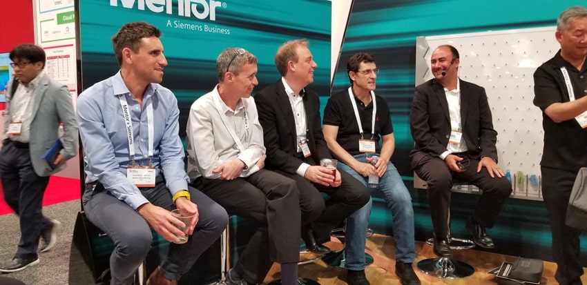
webinar banner2025 (1)

DVCon is coming in February, now is the time to register early

DVCon is coming in February, now is the time to register early
by Daniel Payne on 12-12-2018 at 7:00 am

As 2018 wraps up this month it’s time to start thinking and planning for 2019, and if you work in the Silicon Valley then you’ll want to consider adding the 31st annual DVCon event planned for February 25-28 in San Jose. Surveys have shown for some time now that verification tasks actually take up more time on a SoC project than design does, so it makes sense to find out what’s new for verification engineers through:

  • 39 Technical papers
  • 25 Poster sessions
  • Two Panel discussions
  • Four Tutorials
  • Eight Short workshops


The Accellera Systems Initiative is the sponsor for DVCon, and they grind out the much needed standards so that our industry doesn’t get polarized by proprietary and conflicting software automation approaches.


The Universal Verification Methodology (UVM) can track its history from the Open Verification Methodology (OVM) and even the e Reuse Methodology (eRM) from Verisity back in 2001. Cliff Cummings leads a tutorial on Monday, February 25th all about UVM:

  • “Gain Valuable Insight into the Changes and Features that are Part of the New IEEE 1800.2 Standard for UVM and How to Mae the Most of Them”

Cliff Cummings is President of Sunburst Design, Inc., a company that specializes in world class Verilog, SystemVerilog, UVM Verification and synthesis training. Mr. Cummings is an independent consultant and trainer with 33 years of ASIC, FPGA and system design experience and 23 years of Verilog, SystemVerilog, synthesis and methodology training experience. Mr. Cummings has completed many ASIC designs, FPGA designs and system simulation projects, and is capable of answering the very technical questions asked by experienced design engineers.

For keynote this year you’ll hear about the topic of the “Thriving in the Age of Digitalization” from Fram Akiki, VP Electronics & Semiconductor Industry for Siemens PLM Software. Fram’s background includes 21 years at IBM spanning roles in analog IC design, microprocessor manager and GM. His next 13 years were at Qualcomm as a director of operations, then head of the mobile computing connected products.

There’s a buzz around all things RISC-V, so check out the panel discussion on Wednesday, February 27th entitled, “Verification and Compliance in the era of open ISA- is the Industry ready to Address the Coming Tsunami of Innovation?“. Moderator Mike Demler is a Senior Analyst at The Linley Group, and the panelists include:

  • Emerson Hsiao, Andes Technology
  • Adnan Hamid, Breker Verification Systems, Inc.
  • Rob Shearer, Facebook
  • Simon Davidmann, Imperas Software Ltd.
  • Neil Johnson, XtremeEDA Corp.

Neil Johnson is active on Twitter and his tweets are focused on functional verification.

Networking throughout the conference is available during the Expo on Monday from 5PM to 7PM, then again on Tuesday and Wednesday from 2:30PM to 6PM. View the complete agenda online here, and register online now to get the best prices.

DVCon is the premier conference for discussion of the functional design and verification of electronic systems. DVCon is sponsored by Accellera Systems Initiative, an independent, not-for-profit organization dedicated to creating design and verification standards required by systems, semiconductor, intellectual property (IP) and electronic design automation (EDA) companies. In response to global interest, in addition to DVCon U.S., Accellera also sponsors events in China, Europe and India. For more information about Accellera, please visit www.accellera.org. For more information about DVCon U.S., please visit www.dvcon.org. Follow DVCon on Facebook https://www.facebook.com/DvCon or @dvcon_us on Twitter or to comment, please use #dvcon_us.


56G and 112G SerDes Where the rubber meets the road

56G and 112G SerDes Where the rubber meets the road
by Tom Simon on 12-11-2018 at 12:00 pm

No matter how high the processing capability of a chip, its overall performance is limited by IO speed. This is very similar to a car with low performance tires, a powerful engine will not be able to transfer its energy to the ground effectively. There is quite literally a race going on between core processing and IO speeds for transferring data on and off of chips. AI, autonomous vehicles, 5G and other advances are pushing a never-ending drive to increase data transfer rates.

One interesting area of innovation is in cell towers, where the radios used to sit in a box on the ground and high power RF signals were carried over copper to the antennas. This architecture created power and cooling problems among others. Common Public Radio Interface (CPRI) uses optical cables to carry the digitized RF signal to an RF power amplifier on the cell tower mast. Interestingly when this happened, carriers realized that they could architect their fronthaul to move the Base Band Units (BBUs) to or near the central office. The BBUs rely on high speed data links to get their job done.

Another area of innovation is the advent of Top Rack (TOR) switching. While it shortened the distance from server blades to the data switches, it also comes with a huge upward demand in transfer rates. The pivotal player in all these and many other changes in data transmission paradigms is the ubiquitous SerDes. Big changes have been needed to move from 28G to 56G and 112G and at the same time to limit cross talk and noise as the number of lanes increases.

High speed SerDes are needed not just for short reach connections, the demand for longer lines adds more consideration in SerDes Design. Other requirements for SerDes are back compatibility for lower data rates andlegacy protocols, and the ability to support copper and fiber. eSilicon, a leading provider of complex FinFET ASICs, has put out an interesting article discussing the complexities of designing SerDes for the leading-edge ASICs they deliver. This is in part due to their presence in the networking, AI and 5G markets as silicon a provider.

In their article, they touch on the need to move to PAM4 from the older PAM2/NRZ operation. Multiple bit-levels add complexity, with level detection made more difficult due to switching levels closer to threshold voltages. The leading edge SerDes, operating at 56G and 112G, are both digital and analog, making their design a challenging prospect.

eSilicon also talks about the increased need for on-chip testing and verification features. They have added full speed digital and analog loopback, and also a variety of smart monitoring features. With all this said, eSilicon has 7nm SerDes that are proven in silicon.

Innovation is needed to keep up with the demands for moving data. Ethernet is moving from 100GbE to 400GbE. The data rates for CPRI, mentioned above, are pushing upward from 25Gb/s to 50Gb/s. Back planes and data centers are soon going to be running at 25.6 and 51.2 Tb/s. More data sources, more data consumers, faster networks and high volumes of video and audio real-time data are all pushing technology forward. The eSilicon paper on 56G and 112G SerDes is pretty interesting and worth reading through to get an idea of what is needed to make fast chips move data effectively.


IEDM 2018 – ASML EUV Update

IEDM 2018 – ASML EUV Update
by Scotten Jones on 12-11-2018 at 7:00 am

At IEDM last week Anthony (Tony) Yen, Vice President and Head, Technology Development Centers Worldwide for ASML presented a paper entitled “EUV Lithography at Threshold of High-Volume Manufacturing” authored by Anthony Yen, Hans Meiling, and Jos Benschop. At IEDM I had a chance to sit down with Tony and discuss the paper and the current status of EUV.

Before I summarize my discussion with Tony, I want to comment on where I see EUV in the industry today. Leading-edge logic is going to be the first to implement EUV. Current state-of-the-art logic processes make extensive use of multi-patterning in the Middle-Of-Line (MOL) and Back-End-Of-Line (BEOL) and that is where we will see EUV implemented first. Samsung is the most aggressive in their approach with their first generation 7nm logic process utilizing EUV for 7 layers, Samsung is ramping that process up now. TSMC is offering a second generation 7nm process with 6 EUV layers and that process is due to ramp early next year. Intel has announced their 7nm process will also utilize EUV with a planned introduction date of 2020 although many observers question whether they will meet that date. I have heard the Intel process will use EUV for 6 layers, but it is still early, and I am not sure how credible that forecast is. Samsung and TSMC both have 5nm processes due to begin risk starts in late 2019 with more extensive EUV usage. Clearly EUV is on the threshold of high-volume manufacturing. In my ISS presentation from January 2018 I projected nine hundred thousand wafers will be processed with EUV in 2019 and over two million wafers in 2020. My ISS presentation is available here.

ASML has previously announced the availability of a 250-watt EUV source and that source is now deployed in the field. What is new in the current presentation, is that systems in the field are now maintaining 250 watts. Figure 1 illustrates output power stability at multiple customer systems.

Figure 1. Stable performance at >250 watts on multiple customer systems.

New debris mitigation strategies are improving collector cleanliness. ASML has a goal of only a 0.1% degradation in the mirror per giga pulse of laser output and today is better than 0.3%.

In late 2017 ASML announced their 125 wafers-per-hour (wph) milestone had been reached running source power at 195 watts with 96 steps, 20mJ/cm[SUP]2[/SUP] dose and no pellicle. Early this year throughput was improved to 140 wph at 246 watts with 96 steps, 20mJ/cm[SUP]2[/SUP] dose and no pellicle. Authors note, for logic devices, steps are roughly 110 per wafer and while initial EUV implementation are being done without a pellicle a pellicle is really needed. With a pellicle throughput drops to 116 wph. Figure 2 illustrates the achieved throughput.

Figure 2. EUV throughput.

In our discussions Tony mentioned that the 3400B is shipping today (the system used for the results in figure 2) and that next year the 3400C will start shipping with 170 wph throughput. The 3400C is the same source power as the 3400B but has lower overhead and better lens transmission.

There is also work being done in improving the source power. 410 watts has been demonstrated for short bursts at the factory and ASML believes they can get to 500 watts.

Pellicle development continues. The current polysilicon-based pellicle provides 83% transmission and has now been shown to stand up to 250 watts. Work on a 90% transmission pellicle continues.

CD control and overlay are both excellent and customers are running 36nm pitch today.

The current photoresist of record are Chemically Amplified Resists (CAR). Work with inorganic photoresist have shown single digit nanometer features with improved line edge roughness. Interestingly in his Keynote at IEDM, Samsung Foundry President ES Jung projected that inorganic resists would replace CAR for second generation EUV. Figure 3 illustrates the results of resist screening that shows better LER results with inorganic resist and good line/spaces down to a 20nm pitch although at a high dose of 67mJ/cm[SUP]2[/SUP].

Figure 3. Photoresist comparison.

EUV masks are reflective masks with complex absorber stacks. The height of the stacks creates 3D effects in the mask. There is work under way to find more absorptive materials that would allow thinner layers. Nickel and cobalt offer improved absorption but are difficult to etch. Imec is working on alloys as a possible solution.

ASML is also gearing up to produce high numerical aperture EUV tools as a long-term solution for even finer resolution.

In summary EUV is ramping up today as a 36nm solution for 7nm foundry logic processes. Continued improvement in systems, pellicles and photoresists should carry EUV into the mid-2020s. High-NA systems are being developed to continue further scaling into the late 2020s and beyond.


Changes Coming at the Top in Semiconductor Equipment Ranking

Changes Coming at the Top in Semiconductor Equipment Ranking
by Robert Castellano on 12-10-2018 at 12:00 pm

Semiconductor equipment vendor ranking, which didn’t change much between 2016 and 2017, is undergoing a makeover, as Lam Research, ASML, and Tokyo Electron (TEL) are switching places and top-ranked Applied Materials is getting closer to losing its number one ranking.

Since the 1990s, Applied Materials has been the market leader in the semiconductor equipment space. Previously, Japan’s TEL was the market leader going back to 1989. TEL, which was No. 4 in 2016 is now No. 2 through the first three quarters of 2018. But most important, the spread between the No. 1 and No. 2 companies is rapidly shrinking.

In 2016, Applied Materials was 9.3 share points ahead of Lam Research. In 2017, Applied’s lead dropped to 6.4 share points ahead of Lam. Now, through the first three quarters of 2018, Applied’s lead has shrunk to just 2 share points ahead of TEL.

An important takeaway is that Applied Materials is the only company that lost market share sequentially in each of the time periods, while ASML and TEL were the only two companies that sequentially increased market share in the periods.

More Headwinds Coming
The semiconductor equipment market grew from $41.2 billion in 2016 to $56.6 billion in 2017, an increase of 37.2%. For the first three quarters of 2018, global revenues increased 19.4%. Assuming a growth of 10% for all of 2018, revenues for Q4 2018 should only reach $12.7 billion, down 15.2% YoY from Q4 2017. Chart 1 plots semiconductor market between 2015 and 2018 on a quarterly basis.

Much of the growth in equipment came from Korean semiconductor manufacturers, particularly memory companies Samsung Electronics and SK Hynix. In 2017, Korea represented 31.7% of the $56.6 billion semiconductor equipment sector. Through the first three quarters of 2018, Korea accounted for 29.4% of the global market.

Demand in the server, PC, and mobile markets is weaker than it was earlier in the year, and memory prices are softening in the near term. Because of a drop in average selling prices of DRAMs and NAND, memory companies are pushing out capex spend. Samsung Electronics said the addition of 20,000-30,000 wafers/month of DRAM capacity at the Pyeongtaek plant’s second floor will be postponed to 2020 in order to maintain profitability along with strategic inventory controls.

If margins decrease, Samsung will likely delay a 2019 planned NAND capacity expansion of 30,000 wafers per month on the second floor of Pyeongtaek #1 plant and at its Xian #2 plant to 2020.

While all semiconductor equipment suppliers tout the memory companies among its customers, Applied Materials and Lam Research have high exposure to memory. In its most recent quarter ending October 2018, Applied reported that 60% of its revenue came from the memory sector.

TSMC has also reduced its capital spending outlay for the year, due to weaker than expected sales in iPhones, where it supplies the processor chip, and because the collapse in cryptocurrencies

Applied Materials competes against all equipment companies listed in Table 1 except lithography ASML. ASML is the sole supplier of EUV (extreme ultra violet) lithography equipment. EUV is supposed to slowly replace DUV immersion lithography as the industry moves to the 7nm technology node.

The replacement of DUV immersion by EUV will dramatically reduce deposition, etch, and metrology steps. Current DUV immersion is viable for processing devices with 30nm features. Below that, engineers employ multiple patterning steps as a way of extending the DUV lithography tool. These multiple processing steps are deposition-etch intensively, utilizing equipment from AMAT and LRCX (and others). In other words, semiconductor manufacturers are utilizing multiple patterning processes, requiring extensive use of deposition and etch equipment, to avoid purchasing the extremely expensive EUV lithography equipment.

If we look at Chart 2, using immersion DUV (ArF-1) at the 20nm node there are 13 mask layers, etch of which use multiple dep-etch steps. If we move across the top of the chart, at 10nm there are 18 mask layers, an increase of 50% in the use of deposition-etch steps.

Chart 2

Multiple patterning at the 7nm node, as shown in the bottom left of the chart, requires 27 mask layers. However, by switching to EUV (bottom right) at 7nm, only 14 mask layers are required, similar to the 20nm node with DUV.

As for the terminology, switching from DUV to EUV, the double litho, double etch (LELE) process will be eliminated while ArF-I (immersion DUV) would continue to be used for the self-aligned double patterning (SADP) and self-aligned quadruple patterning (SAQP) processes. Most importantly, half the processing steps will be eliminated.

A combination of all these headwinds are significant detriments to the sustained growth of the semiconductor equipment market in 2019. According to The Information Network’s report “The Global Semiconductor Equipment: Markets, Market Shares and Market Forecasts,” that means global equipment revenues could drop 8%.


IEDM 2018 Trip Report!

IEDM 2018 Trip Report!
by Daniel Nenni on 12-10-2018 at 7:00 am

Hello, my name is Daniel Nenni and I am a semiconductor conference addict. I just can’t seem to get enough. The semiconductor ecosystem is very wide now and moves so quickly it is nearly impossible to keep up without constant conference attendance. As a SemiWiki contributor not only do I get free conference passes, I get access to people and materials that help feed my insatiable appetite for semiconductor information. The world really does revolve around semiconductors and now me personally since I know all that is semiconductor, absolutely.

Premier SemiWiki blogger Scott Jones also attended IEDM and will have more detailed blogs coming soon.

About IEDM
With a history stretching back more than 60 years, the IEEE International Electron Devices Meeting (IEDM) is the world’s pre-eminent forum for reporting technological breakthroughs in the areas of semiconductor and electronic device technology, design, manufacturing, physics, and modeling. IEDM is the flagship conference for nanometer-scale CMOS transistor technology, advanced memory, displays, sensors, MEMS devices, novel quantum and nano-scale devices and phenomenology, optoelectronics, devices for power and energy harvesting, high-speed devices, as well as process technology and device modeling and simulation. The conference scope not only encompasses devices in silicon, compound and organic semiconductors, but also in emerging material systems. IEDM is truly an international conference, with strong representation from speakers from around the globe.

As I mentioned before, IEDM is the premier semiconductor process technology conference. This year the theme is Device Breakthroughs from Quantum to 5G and Beyond. One of the more interesting topics to me was Interconnects to Enable Continued Scaling with papers from ARM, IBM, IMEC, UT Austin, GlobalFoundries, Stanford, and AMAT. This is a must read for those of you who think Moore’s Law (which is actually an observation) and semiconductor scaling is at an end, because it is not, not even close.

There was also an interesting session on 3D integration: High Density Stacked FinFETs and 3D integration of 2D memory. Memory technology was a major focus (especially MRAM), and rightly so, but I did not have time for it unfortunately. Photonics also made it into the program which is a good thing. We track photonics related content on SemiWiki and have seen a significant rise in content and readership in 2018.

Based on my time mingling amongst the crowd I was happy to see a lot of young faces. IEDM is clearly doing a great recruitment job. The old guard, me included, always wonders who will replace us as time goes by. Based on what I saw this week I think we are in good hands, no problem.

The one criticism I do have is the exhibit hall. It was pretty lame to which I say why even have one at all? Seriously, a complete waste of precious space. If a vendor wants exposure make them write papers and rent hotel suites for more intimate conversations. Leave the exhibit halls to the user group meetings and less technical conferences like CES, my opinion.

We can have an IEDM discussion in the comments section if you like. I have copies of the presentations and conference proceedings for reference.


GM: Stop the Downsizing!

GM: Stop the Downsizing!
by Roger C. Lanctot on 12-10-2018 at 7:00 am

General Motors CEO Mary Barra is known for a number of quotes one of which is: “My father was a die maker for 39 years, so I had a basic understanding of the automobile industry and what the manufacturing world was like, just from the opportunity to spend time with him, just talking, because he was a car buff.” One has to wonder what Mary’s dad would have so say about the latest news out of GM.

Two major press events preceded this year’s Los Angeles Auto Show and AutomobilityLA. The first event arrived the Friday before the Show following the Thanksgiving holiday bringing news of a government report revealing catastrophic human-influenced climate change. On Monday, General Motors announced its plans to idle or close five plants (four in the U.S. and one in Canada), layoff 14,000 workers and terminate five sedans: the Chevrolet Cruze, Volt and Impala, Buick LaCrosse and Cadillac CT6.

The catastrophic climate report was notable for its release occurring on a Friday in the middle of a holiday. Journalists commented that the decision was clearly taken by the Trump administration to dump the report on a Friday to ensure that it received as little attention as possible.

In contrast, the GM announcement came on the Monday following the holiday weekend and preceding the L.A. Auto Show guaranteeing widespread press attention and analysis. The decision was clearly a calculated one as GM’s stock price rose nearly 5% on the news, as investors rewarded GM’s apparent fiscal prudence.

Unfortunately, the decision to release the announcement on Monday also revealed GM’s priorities. In spite of anything GM’s leadership might have to say about its employees or its customers, the top priority is clearly investors.

In spite of GM’s best efforts, though, the stock hasn’t budged much from its IPO price. The latest bump, like those that have preceded it, will rapidly fade and fall.

GM’s massive market retreat has been underway since the government bailout and bankruptcy approximately 10 years ago. At that time GM, along with Chrysler, used the opportunity of bankruptcy to justify the termination of 3,389 dealers.

Terminating dealers seems like a counter-intuitive strategy for a company planning to emerge from bankruptcy and needing to sell more cars. But as Tammy Darvish, author of “Outraged,” describes it, the move was clearly intended to reduce inter-dealer competition and goose profit margins.

GM has continued to pursue higher vehicle prices and profits by dialing back on incentives. It remains unclear as to precisely how sustainable that strategy will be. GM’s profit-driven market manipulations have plunged the company to fifth place globally based on vehicle production – well behind Hyundai and slightly ahead of Ford.

The pursuit of profit has contributed to decisions to close plants in Australia, Indonesia, India and Russia while pulling out of the European market by selling Opel to PSA. Other market exits included India, South Africa, and Russia.

The company has also bought back $10B in stock since 2015. Investors have questioned the purpose or wisdom of these buybacks – normally done to increase the stock price – since the stock has shown little movement.

Meanwhile GM has been sinking hundreds of millions of dollars into Cruise Automation and launching the Maven car sharing service. The company line on this mix of exits and investments is that GM is investing in the future, preparing for a shared, autonomous, electric vehicle future.

But it is difficult for the company to escape the logic that its strategy of focusing on profitable operations and cutting off unprofitable ones directly contradicts its investment strategy of pouring money into ventures with uncertain prospects. Both Maven and Cruise are facing mixed results with Maven expansion plans on hold and Cruise failing to meet critical milestones on the path to autonomous operation.

The biggest and most dubious claim of all at GM – and it is one that is shared by Ford Motor Company – is the company’s almost complete exit from the passenger car market – joining FCA and Ford in focusing on SUVs, crossovers and pickup trucks. GM, like its Detroit competitors, blames a lack of consumer interest in passenger cars and a correlated decline in sales.

GM, Ford and FCA make much more money selling SUVs, crossovers and pickups than they do selling cars. So it is logical to want to make more of these large vehicles and less of smaller, passenger vehicles.

This myopic profit-driven strategy is effectively painting the three Detroit OEMs into a marketing corner. A trucks-and-SUVs-only strategy makes all three of these auto makers more vulnerable than ever to imports and domestically manufactured trucks and SUVs from import makes.

What is perhaps most stunning, though, is GM’s decision to terminate the Volt. It’s easy to make the case that sales of the Volt failed to meet the 30k/month goal originally intended, but it is also easy to make the case that GM never fully funded the market funnel to drive demand.

Car makers often paint themselves as the sad victims of market forces and lagging demand. The reality is that car makers spend billions of dollars telling consumers what cars they “want” or “need.” Consumer demand is not occurring in a vacuum.

The Volt extended range EV has consistently produced some of the most amazing customer satisfaction scores ever seen by General Motors. Volt evangelists are legion, yet GM has somehow failed to embrace these brand ambassadors and leverage them to build a stronger footing in the EV market.

Now GM is terminating the Volt – or so it seems. Such a move represents an extraordinary destruction of market value comparable only to GM’s sales of Opel to PSA.

It’s not too late for GM to turn in the direction of the skid and get itself back on track. Of course, the Trump administration won’t make that easy with threats of suspending GM’s EV subsidies and slapping tariffs on cars imported from GM factories in China.

It’s time for GM to take a greater interest in its customers, its dealers, and its workers and, for at least a quarter or two, tell Wall Street to take a hike. It’s time to get back to basics – get back to the product.

With the passing of FCA CEO Sergio Marchionne and the ousting of Renault-Nissan-Mitsubishi Chairman Carlos Ghosn the stage is clear for a real game changer, GM’s Mary Barra. It’s time for Barra to take her place as the leading voice of the global automotive industry – an industry that needs a more inspiring vison than the prospect of endless downsizing that has unfolded under her guidance thus far.

Another one of Mary Barra’s noted quotes is: “My definition of ‘innovative’ is providing value to the customer.” Right on, Mary.


Volvo: Car-less is Better Than Clueless

Volvo: Car-less is Better Than Clueless
by Roger C. Lanctot on 12-09-2018 at 7:00 am

Sweden has embraced the movement toward a cashless society with banks no longer taking cash deposits and retailers, like Ikea, experimenting with cashlessness. Perhaps taking a cue from the Swedish financial sector, Volvo Cars last week revealed its plans for a car-less stand at this week’s L.A. Auto Show – and the co-located AutomobilityLA.

Volvo’s announcement shines a light on Swedish thought leadership at a time when competing car companies babble incoherently about so-called “mobility.” The car-less stance is in keeping with Volvo’s visionary past which emphasized safety before it was sexy and years-ago gave a yet-unmatched promise to accept crash liability once autonomous driving is achieved.

From General Motors to Ford Motor Company to Toyota and Volkswagen, auto CEOs struggle to redefine their missions in an industry on the cusp of massive disruption. Simultaneously, politicians are at war with cars, car owners and car makers around the world (water cannons and tear gas in Paris this past weekend along over higher fuel taxes) putting pressure on car makers to pave the path to peace.

For Volvo, that path means exploring alternatives to vehicle ownership along with developing creative ways of using cars. “We are trying to shift our focus from doing what we have done for the last 90 years,” Volvo Senior Vice President of Corporate Strategy Marten Levenstam, purported mastermind behind the Volvo exhibit, told Automotive News.

The Automotive News reported that Volvo will use its display area for interactive demonstrations of connectivity services, such as in-car delivery, its vision for autonomous driving and its Care by Volvo vehicle subscription service. The stand will also show Volvo’s plans for car sharing.

Volvo’s CEO, Hakan Samuelsen, added that the company wants to move beyond simply building and selling cars. In its quest for redefinition, Volvo has partnered with Amazon, Google, Nvidia, Luminar and Zenuity.

It is difficult to overstate the significance of Volvo’s move coming at the L.A. Auto Show. At a time when car companies are reconsidering their participation in car shows in Paris, Frankfurt, Geneva and elsewhere, the U.S. continues to host half a dozen prominent car shows including Detroit, Los Angeles, New York, Chicago and Washington. The Los Angeles and Detroit events are the largest and most popular and those cities each have a unique relationship with cars.

Detroit, Motown, is seen as the epicenter and birthplace of the North American automotive industry with General Motors’ headquarters located downtown and Ford and FCA based in the suburbs. L.A., on the other hand, is the ultimate embodiment of North American automotive culture blending Hollywood, and hundreds of miles of freeways and ocean-front beaches.

Detroit and L.A. also share a tortured relationship with public transportation. L.A., at least, has the benefit of mass transit including rail running above and below ground to go along with an extensive bus transit system. Detroit has little or no mass transit for stitching together the city with surrounding suburbs. In fact, Detroit crashed out of contention for Amazon’s HQ2 sweepstakes thanks in large part to its lack of mass transit infrastructure.

General Motors bears more than a little of the blame for having cutoff Detroit’s transit oxygen. Now, would be a good time for the General to reverse course especially in the context of the current “mobility” push.

The birthplace of the car in North America, faces the prospect of becoming an automotive cemetery due to the city and the State of Michigan’s inability to craft an attractive transit program better integrating the city with the suburbs. In spite of GM’s prominent downtown location, it is Dan Gilbert, CEO of Quicken Loans, also headquartered downtown, who has taken a leadership role in fostering the fledgling Qline trolley limping along Woodward Avenue.

Disruptive times demand bold moves. Volvo may not have all the answers, but the company is making a statement in L.A. that the time has come to think differently about cars and transportation. (Even Tesla Motors CEO Elon Musk has taken on the transit challenge with his Hyperloop and Boring Company initiatives.)

It is clear that no single company, in fact no company, has the answers today. But the challenge of moving people into and around cities and suburbs in the safest, cleanest and most efficient manner possible is the goal. It may require cars or it may require something entirely different. Volvo is pointing the way to new possibilities. Car companies need to get into the game.


Could China Conflict Curtail Chip Comeback? Part 2

Could China Conflict Curtail Chip Comeback? Part 2
by Robert Maire on 12-07-2018 at 12:00 pm

In our recent note sent several days ago we suggested that the China conflict would come back to haunt the US chip industry. From a stock perspective we suggested taking short term gains from a recent bounce back off the table. Both ideas turned out true, but way faster than we had thought! Not only have investors figured out that the trade truce was hollow but just to make sure, the US had Huawei’s CFO arrested in Canada.

Given that Meng Wanzhou, who was arrested, was not only the CFO but also the daughter of the founder of Huawei, China’s biggest tech success story, as well as a high ranking female, this is not just a slap in the face but rather Trump personally spitting in Xi’s face.

Guilt or innocence is not the issue as we think Huawei is very guilty. The ongoing joke from 15 years ago, which was no joke, was that Huawei routers when booted up would say Cisco on the display as all the code was stolen from Cisco. Huawei even admitted in court to stealing some of Cisco’s code, it was that blatant. We are also very sure that Huawei could care less if their products containing US semiconductors are sold to bad actors around the globe, much as ZTE did.
Yes, Huawei is very, very guilty but the timing of the arrest is the question not the guilt. Its very personal now between Trump & Xi.

If ZTE doubled China’s resolve to get big in the semiconductor business, Huawei just tripled it.

The next question is whether the administration did this on purpose to piss off China and play the role of “disruptor in chief” or it was just just a question of one hand not knowing what the other was doing. Maybe if its the latter the Chinese could brush it off to stupidity and not react as badly….but we’ll never know.

We would now put the odds of a “good” trade resolution at less than 50%. By good we mean tariffs going away and not giving up everything.

Payback
We would not be surprised if there were some further retaliation against the US tech industry. If we were the CEO/CFO of Micron, we probably wouldn’t want to be traveling anywhere near China for fear of being yanked off a plane for patent infringement, or some other charge.

Whereas the trade truce was likely good for KLAC/ORBK, China could now squash the deal as Huawei payback as it has clearly admitted that M&A approval is only political in nature. Responding in a non-tariff way would allow the Chinese to say they are respecting the truce just like the US.

Reconsidering QCOM/NXP was a joke as everyone understands it was dead and buried.

American Sniper
The arrest of Meng Wanzhou is like a US sniper taking out a North Korean general across the DMZ two days after the truce in 1953…..they might not be happy with us. We don’t think this is a case of a lone sniper not getting the ceasefire message, we think this was calculated on the US part.

Do we even make it to 90 days?
If this is the start of the ceasefire, how much worse can it get? China has now publicly played down what ever was not agreed to in South America. We think the Chinese position got very much more entrenched over the Huawei arrest, and will make compromise very, very difficult.

It all comes back to the semiconductor industry
As we have said for a long time, all roads in trade lead back to the chip industry. The core issue here are the US chips in Huawei products . China needs desperately to be independent of the US to get rid of this issue once and for all.

Chip equipment is at the very core of being independent. China desperately needs chip equipment to get their own chip production up. Jinhua / UMC / Micron was just the beginning of an ongoing struggle behind the public trade war.

The only true leverage the US has is to stop export of semiconductor equipment to any Chinese fab, foreign or domestic, which will choke off China’s oxygen supply. That may become the ultimate “nuclear option” if trade talks go south from here.

The stocks
We would still avoid the stocks as we don’t like where things are headed (in a hurry). We think the downside beta remains higher than the upside beta in the trade issue and the tech industry could wind up with the short end of the stick if there were a bad agreement.

The administration seems more focused on soybeans and cars than chips and technology which is the real underlying issue. We would not be surprised for the administration to announce a “win” in trade on selling the Chinese more soybeans and cars only to cave on chips and technology which is less well understood.

Either way, its going to be rocky for a while with the stocks in a volatile pattern. We would rather watch from the sidelines.

Also Read: Could China Conflict Curtail Chip Comeback?


ARM Answers Server Doubts

ARM Answers Server Doubts
by Bernard Murphy on 12-07-2018 at 7:00 am

At ARM TechCon this year, the company announced the Neoverse brand targeted to infrastructure, contrasting with the Cortex brand we are familiar with for edge devices such as smartphones and IoT devices. Cortex was already used in infrastructure, in networking, base stations and the like but Neoverse splits the infrastructure line of business from the edge line of business, including a roadmap for a dedicated family of processors.

Few would dispute that ARM has a big footprint in communication infrastructure, but the high end of the Neoverse plan, as presented at TechCon, is in servers. Here many would argue that the evidence for progress was less compelling. Servers from HPE (based on Cavium/Marvell processors) and Ampere for example show some progress, and ARM asserts a million units have shipped this year. But Qualcomm dropping out of servers was widely read as a negative and some of us had started to wonder if ARM plans for servers were more hope than substance. ARM may not be Apple or Samsung, but they’re at a scale where a million units in a year is no longer particularly exciting. Where were the big wins?

ARM answered that question definitively when AWS (Amazon Web Services) very recently announced the immediate availability of Neoverse-based servers in their instance lineup. The Graviton processor at the heart of these servers was developed by Annapurna Labs (wholly owned by AWS). This news is compelling on a couple of levels. First, ARM-based servers are part of the AWS instance line-up (EC2 A1 instances). That’s about as a big a win for ARM servers as you can hope to find. Second, AWS developed these processors themselves. That certainly helps with cost and power, but more importantly it signals expanding need to differentiate in the cloud providers. We knew about this around the edges: GPUs for deep learning and ASICs/FPGAs for network optimization and software-defined storage. Looking for advantage in custom servers over commercial solutions takes differentiation to a new level and is likely to cause some disruption in the value-chain.

I talked with Mohamed Awad, VP of the infrastructure line of business at ARM to get more information on why the ARM-based servers work in the AWS lineup and how this may evolve over time. Mohamed acknowledges that lower cost instances in AWS EC2 services are a very visible advantage to cloud users, especially for ARM-based workloads. I have no doubt also that AWS is attracted to ARM’s end-to-end IoT strategy which should drive lots of traffic to their cloud. Why not make that as easy as possible?

I had to ask about performance. There are a number of comparisons of ARM-based server performance (EC2 A1 and Ampere for example) which show these are not as fast as high-end Intel Xeon or AMD Epyc servers. Are ARM-based servers intended mostly to serve ARM-generated traffic and the low-end of the cloud market?

Not at all, according to Mohamed. I’m probably not alone in thinking of datacenters as homogenous ranks of high-end server blades with maybe a few special-case oddities like GPUs sprinkled around. But Mohamed told me that’s already changing. Cloud workloads are not homogenous and there are multiple ways competitive providers can provide services to optimize those workloads, beyond deep-learning, network and storage accelerators. Less familiar may be support for web services (more data throughput than compute intensive, but need to serve many clients in parallel), containerized microservices (a popular trend virtualizing components of a larger service) and applications caching (like caching inside a device but here caching state for an application across many devices). Could you do all of this with Xeon or Epyc servers? Probably. Could you do it more cost-competitively, and maybe better in distributed compute throughput with custom servers? Absolutely.

The EC2 A1/Graviton instance is based on the ARM Cosmos platform, in turn based on the A72 and A75 cores. Following this ARM plan to introduce, on a yearly beat, the Ares, Zeus and Poseidon architectures, each of which they intend will show ~30% incremental improvement in performance, along with new features. Can they catch up with the high-end Intel/AMD processors? Who knows, but clearly that isn’t a necessary goal. There seems to be plenty of compute share they can grab in these rapidly evolving datacenter architectures.

Finally, I asked Mohamed about the other cloud providers – Microsoft Azure, Google Cloud and others. He wouldn’t tell me, but I have seen indications elsewhere that similar programs are underway. And frankly, if you were running those operations and you knew AWS were working on an added edge based on ARM-based servers, wouldn’t you be talking to ARM too?

Looks like ARM knew all along what they were doing in servers, they just didn’t tell us. And we spent all our time looking in the wrong direction.


Samsung IEDM 2018 Keynote and the Foundry Business

Samsung IEDM 2018 Keynote and the Foundry Business
by Daniel Nenni on 12-06-2018 at 12:00 pm

IEDM is a premier semiconductor conference so it was certainly appropriate for Samsung to do the keynote since they are the largest and one of the most innovative semiconductor companies in the world, absolutely.

Samsung is also one of the more interesting semiconductor companies since they do it all: chip design, semiconductor manufacturing, consumer electronics, and foundry services. Having worked with Samsung many times throughout my career, which included numerous trips to Seoul, I will offer my experience, observation, and opinion, but first let’s talk a bit about the keynote.

Dr. ES Jung, President and GM of the Samsung Foundry business, did the keynote. He started with a joke stating that ES stands for engineering samples which got quite a few laughs, especially from me. ES is a career Samsung employee (he started in 1985) and has spearheaded research and development of advanced logic and memory process technologies and now leads foundry services.

Here is the abstract for his presentation. Remember, IEDM is a conference not a trade show so everyone does papers with abstracts and references:

4th Industrial Revolution and Foundry: Challenges and Opportunities
Abstract—Semiconductor has been the key enabler in the advancement of electronics for the past 50 years. With the coming of 4th industrial revolution, semiconductor will continue to play an even greater role as we invite a wide variety of new applications into our lives, including smart cars, smart factories, artificial intelligence, data centers, robots, etc. Such importance of semiconductor is attributed to its unique ability to copy and create everything human beings imagine. In this paper, the roles of foundry in the 4th industrial revolution, as the entity to turn ideas into reality along with electronic design automation (EDA), intellectual property (IP) vendor, and outsourced semiconductor assembly and test (OSAT) companies, as well as the need for global open innovation to overcome imminent challenges will be discussed.

I also have the slides but I’m not able to share them due to conference guidelines. It is a shame too because there are some very interesting ones. The presentation is in three parts: Industrial Revolution and Semiconductor History, Foundry, Challenges and Opportunities for Innovation.

I’m a big history fan because you really need to know how you got to where you are today to better plan for where you are going tomorrow, right? We have all seen the semiconductor history slides and know semiconductors are a critical part of modern life but it’s nice to be reminded before you get into the really interesting foundry and innovation slides.

With Samsung we have come full circle with the foundry business which started when IDMs had extra fab space that they rented out. Unfortunately, when IDM fabs filled up, the foundry business was shelved, which is what happened to Intel Foundry and is now quietly but officially shut down. The rest is history, pure-play foundries took over and have dominated the fabless chip business for more than 30 years now.

An important part of the foundry business was the ability to multi source to get the best pricing and availability. I remember being involved with a design that was sourced to four different 40nm fabs (TSMC, UMC, SMIC, and Chartered). Some fabless companies were loyal to one fab but that was rare. Now multi sourcing one design to multiple fabs is not possible. In fact, at the leading edge you now only have two foundry choices (TSMC and Samsung). You can certainly use both fabs for different designs and moving forward many companies will do just that, my opinion.

This brings me to the realization I had watching the Samsung keynote. In my dealings with Samsung the most important thing I learned is that they do not give up which is critical in the foundry business. I remember many years ago Samsung told me during one of my visits that they were going to be the number one semiconductor company in the world and here they are. Today, if Samsung told me they were going to be the number one foundry in the world I would not bet against it.

Currently TSMC ($32B+) is the number one foundry by a very large margin with GF ($6B+), UMC (>$5B+), Samsung (>$5B+), and SMIC $3B+) barely visible in the rearview mirror. My prediction today is that Samsung and TSMC will share the majority of the foundry business in the coming years with UMC and GF joining the ranks of the boutique foundries. SMIC is the big question since they have the upper hand in the Chinese market but lack the leading edge innovation. Remember, China buys more chips than the rest of the world and that number will only increase in the years to come, my opinion.

So, my prediction for leading edge wafers in 2025 is that TSMC will have 60% market share and Samsung 40%. I will make my case in the comments section.