RVN! 26 Banner revised (800 x 100 px) (600 x 100 px)

Automating Timing Arc Prediction for AMS IP using ML

Automating Timing Arc Prediction for AMS IP using ML
by Daniel Payne on 10-16-2019 at 6:00 am

Empyrean, Qualib-AI flow

NVIDIA designs some of the most complex chips for GPU and AI applications these days, with SoCs exceeding 21 billion transistors. They certainly know how to push the limits of all EDA tools, and they have a strong motivation to automate more manual tasks in order to quicken their time to market. I missed their Designer/IP Track Poster Session at DAC titled, Machine Learning based Timing Arc Prediction for AMS Design, but the good news is that I did attend a webinar from Empyrean that covered the same topic.  Anjui Shey from Empyrean was the webinar presenter and he talked about Qualib-AI, an EDA tool with AI-powered timing arc prediction for AMS IP blocks.

First off, let’s look at some of the AMS IP modeling challenges:

  • Complex IP creates higher design risks
  • Difficulty modeling AMS IP
  • A missed timing arc can lead to chip failure
  • Toggling within an IP changes thermal condition and timing
  • Process variation creates a large number of PVT corners

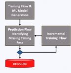
Empyrean updated their Qualib library analysis and validation tool to use ML, creating the Qualib-AI tool as shown below:

A timing arc is where you define a timing dependence between any two pins of an IP block. CAD groups are tasked with adding timing arc information for each IP block, and for AMS designs this has been a time consuming manual effort that is error prone.

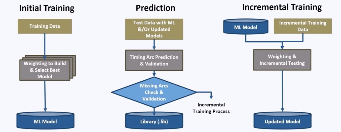
There are three flows used in this methodology for timing arc prediction: Initial Training, Prediction, Incremental Training.


The training data comes from previous AMS cell libraries. Benefits to using ML for predicting timing arcs include:

  • Higher coverage of predicted timing arcs
  • Better accuracy for timing type predictions
  • Fewer false positives and negatives, saving time

NVIDIA ran initial training on 411 IP blocks and then used prediction on a set of 30 new IP blocks as shown below, automatically finding 6,774 arcs and identifying 15,124,093 non-arcs:

The CPU runtimes for initial and increment training plus prediction were pretty fast at about one hour, a much shorter amount of time had the engineers done manual timing arcs:

With an incremental training flow there were three improvements in predicting the timing arcs:

  • Number of false positives decreased 9x, number of false negatives decreased 40X
  • Reached 99.6% coverage to predict timing arc with timing type
  • Reached 98.96% accuracy to predict the timing type

After incremental training there were fewer than 100 false positives for the engineers to review, which is a manageable amount compared to previous efforts.

Summary

Engineers creating AMS IP blocks can now automate how timing arcs are created, saving them time and reducing the risk of a silicon re-spin. Libraries of AMS blocks can be run through this flow to uncover missing arcs, thus improving the quality of the library. The number of false positives has been decreased greatly, and run times for this approach are acceptable.

Watch the archived webinar video here.

Related Blogs


Cadence and Green Hills Share More Security Thoughts at ARM Techcon

Cadence and Green Hills Share More Security Thoughts at ARM Techcon
by Randy Smith on 10-15-2019 at 10:00 am

On Wednesday, October 9, 2019, I had the pleasure of spending the day at ARM Techcon at the San Jose Convention Center. In the morning, in addition to getting some sneak peeks into the exhibitor area, I attended some of the morning keynote presentations, which focused on artificial intelligence (AI) and machine learning (ML) topics. Those were great presentations and a special thanks to the ARM marketing team for the high-end production value. Next, I was off to see some of the technical sessions, giving me a chance to get back to my EDA and verification roots.

I attended a joint presentation by Frank Schirrmeister of Cadence and Joe Fabbre of Green Hills titled, Pre-silicon Continuum for Concurrent SoC, Software Development and Verification for Safety and Security Critical Systems. At the Cadence Automotive Summit just this past July 30th, I also saw a presentation from Dan Mender, Green Hills Software’s VP, Business Development called Addressing the State of Safety and Security in Today’s Autonomous Vehicles System Designs. These two presentations have demonstrated to me just how serious these two companies are about working together to solve the critical requirement of system security. You can see my blogs from the Cadence Automotive Summit here and here.

One common message from both presentations is the simple theme that you cannot have safety if you do not also have security. The point is that no matter how much you work on safety, a system that is vulnerable to a malicious attack, will not remain safe. This concept applies to all types of systems, not just automotive. Working with Cadence and Green Hills allows a system architect to utilize security measures in both the hardware and software design. One nugget I saw in the presentation was the theme shared by both companies to simplify architectures, specifically, “Separation of critical components with an emphasis on simplicity for critical components is key.”

As we all know, the earlier you find a design flaw, security gaps, and other bugs, the less expensive it is to fix. This perception increases the importance of two concepts – Hardware/Software Co-Verification, and Virtual Platforms. These are areas where Cadence has succeeded and has a thorough product portfolio to support its customers.

As the diagram above shows, several different techniques can be applied to co-verification as we move through the different design stages. You will find the largest number of bugs at the beginning of the design process, and the rate of finding bugs should decrease over time. But these later bugs are still important as they may not show up until the design process reaches its more refined stages. Test coverage and test suites will also get more thorough in time, and you will want to use these tests at the most refined version of your system available at that time. The full range of Cadence verification products can solve that for you.

The presentation also reviewed some of the technology integration points as they are developed and optimized through the Cadence collaboration with Green Hills. For instance, the Green Hills Hypervisor and RTOS technology Integrity – focused on safety and security – can run on the Cadence dynamic verification engines. The software is compiled using safety-aware, certified compilers, and it can be debugged using the Green Hills Multi IDE, which is connected via standard interfaces like JTAG. As an example integration, a virtual platform using Arm Fast Models was shown to boot Linux and get debugged using the Green Hills Multi IDE.

The earlier you can do software development, the more time you will have to find and fix bugs – and security flaws are just that, bugs! Being able to run software testing on virtual platforms rather than waiting for functional silicon is a huge benefit. You will only be able to find some security flaws when running software on a model of the hardware or the hardware itself. Cadence’s Virtual System Platform enables you to start testing your software long before RTL or prototypes of the hardware are available. The virtual system platform can be combined with other parts of the Cadence  System Development Suite, such as Cadence’s emulation and prototyping products, to give you a fast, reliable environment for doing early software development and validation.

This session was one of several very useful presentations at ARM Techcon. If you missed it this year, make sure to put it on your schedule for next year. If you sign up to be notified when ARM TechCon 2020 registration opens, ARM will give you a $100 discount on the regular price of an All-Access conference pass for the 2020 event.


Formal in the Field: Users are Getting More Sophisticated

Formal in the Field: Users are Getting More Sophisticated
by Bernard Murphy on 10-15-2019 at 5:00 am

Formal SIG 2019 meeting at Synopsys

Building on an old chestnut, if sufficiently advanced technology looks like magic, there are a number of technology users who are increasingly looking like magicians. Of course when it comes to formal, neither is magical, just very clever. The technology continues to advance and so do the users in their application of those methods. Synopsys recently hosted an all-day Special Interest Group event on formal in Sunnyvale, including talks from Marvell and others, with a keynote given by my fellow author Manish Pandey and Pratik Mahajan. A number of points captured my attention.

Regression with ML

Nvidia talked about regressing formal runs. This started with an observation that complexity is growing in many directions, one of which is arbiters, FIFOs and state machines all talking to each other. Proving you have covered all the bases quickly runs out of gas in dynamic verification of possible interactions between these systems. In fact, even trying to do this through bottom-up property checking is dodgy; who knows what interactions between subsystems you might miss? So they chose to go with end-to-end (E2E) property checks to comprehensively cover all (necessary) systems in proving.

The problem in that idea is proof convergence. Taken together these are very big state machines. Nvidia turned to the standard next step – break each property down into sub-properties (with assume-guarantee strategies for example). The sub-properties are easier to prove in reasonable time, but each requires its own setup and proving, and these E2E goals generate lots of sub-properties. This generates so many sub-proofs that resource competition with other forms of verification becomes a problem.

Their next refinement was to apply ML capabilities (RMA) available with VC formal, both within the tools and in learning between tool runs, to accelerate runs and to reduce resource requirements. They do this initially in interactive convergence and subsequently in regression runs. In both cases the advantages are significant – order of magnitude improvements in net run-times. Clearly worthwhile.

Proof Using Symbolic Variables

Microsoft talked about validating a highly configurable interrupt controller IP more efficiently. Their approach was based on connectivity checks for each configuration; they found that in a previous rev this expanded to tens of thousands of assertions and took 2 days to completely validate. In a newer and naturally more complex rev of the IP this grew to 2.5M assertions, the complete proof wouldn’t converge, and initially they were forced to reduce the scope of proving to a sample set, not exciting when the goal had been to demonstrate complete proofs.

Then they got clever, looking at the symmetries in the problem and using symbolic variables for key values in the design, each constrained to lie within its allowable range. This isn’t entry-level formal (you have to think about what you’re doing), but it is very powerful. Proof engines will prove over an assumption that such variables can take any allowed value within their constrained ranges, so the proof is complete but can operate on effectively a smaller problem. That allows for much faster run-times. The large example (which wouldn’t complete before) now ran in 24 hours. Out of curiosity they re-ran the smaller example that previously took 2 days; this now ran in 15 minutes.  As everywhere in verification, clever construction of a testbench can make huge difference in runtimes and in coverage.

Sequential equivalence checking

This (SEQ) is the standard way to verify clock gating, however the Samsung speaker talked about a number of applications beyond that scope: validating for RTL de-featuring (where you turn off ifdef-ed functionality), sequential optimizations (e.g. moving logic across flop boundaries to improve timing), shortening pipeline stages and power optimizations, all verification tasks you can’t pull off using conventional equivalence checking. Given the extended nature of such checks they can be a little more involved than conventional checking. He talked about multiple capabilities they are able to use in VC Formal to aid in convergence of proofs – orchestration, CEGAR memory and operator abstraction and specialized engines. Overall this enabled them to find 40+ RTL bugs in 5 months. He added that 40+% of the bugs were found by new hires and interns, highlighting that this stuff is not only for advanced users.

Datapath Validation

Lastly, Synopsys have now folded their HECTOR datapath checker under VC Formal Datapath Validation (DPV) App. This employs transaction-level equivalence to validate between a C-level model and the RTL implementation. Datapath elements for a long time were one of those areas you couldn’t use formal, so this is an important advance. Marvell talked about using this capability to verify a number of floating-point arithmetic function blocks. In standard approaches, whether for simulation or “conventional” formal, the number of possibilities that must be covered is exponentially unreachable.

The Datapath Validation App works with Berkeley SoftFloat models, widely recognized as a solid reference for float arithmetic. This team used those models in DPV equivalence checking with their RTL implementations and found a number of bugs, some in the RTL and some in the C++ models and added that they subsequently found no bugs in simulation and emulation. This suggests to me that this type of verification is going to see a lot of growth.


Interested users can request the material from VC Formal SIG from their Synopsys contacts. You can checkout VC Formal HERE.


Free webinar – Accelerating data processing with FPGA fabrics and NoCs

Free webinar – Accelerating data processing with FPGA fabrics and NoCs
by Tom Simon on 10-14-2019 at 10:00 am

FPGAs have always been a great way to add performance to a system. They are capable of parallel processing and have the added bonus of reprogramability. Achronix has helped boost their utility by offering on-chip embedded FPGA fabric for integration into SoCs. This has had the effect of boosting data rates through these systems by eliminating data movement through IOs and off chip connections.

Achronix is now smashing down the next barrier to SOC performance with the addition of a Network on Chip (NoC) that works in conjunction with the FPGA fabric and all the other elements of the SOC. To help explain how this works, Achronix is offering a free webinar on how data processing algorithms can be accelerated by combining embedded FPGAs and NoCs.

The webinar presenter will be Kent Orthner, Achronix, Senior Director, Systems. He has a long and varied career in both FPGA and NoC technologies. At Achronix he is a key contributor to leading edge FPGA architecture and SoC integration. With his level of expertise this promises to be extremely informative.

NoCs offers many advantages for FPGA based SoC design. Using Achronix’s novel approach, NoC access points can be placed throughout the FPGA fabric to facilitate high speed data transfers within and to outside of the SoC. Off chip memory can be accessed efficiently and PCie ports can also be utilized in the same way. The NoC pipes offering 512Gbps are located as needed in the FPGA processing array. Additionally, there are specialized data transfer modes for 400G Ethernet ports.

Combined SoCs that utilize Achronix NoC and embedded FPGA processing arrays should offer formidable performance. This webinar looks like it could be useful for engineering management, SoC architects and system designers. The webinar, “Accelerate Data Processing Algorithms using FPGAs with 2D Network-on-Chip”, will be offered on October 24th at 10AM Pacific Time.

More information and the registration page can be found here. I am a frequent attendee of webinars because they offer a painless and quick way to keep up on the latest trends in semiconductor technology. I am definitely looking forward to this one. Achronix has consistently been an innovator and looks to be continuing that trend.


Response to IP’s Growing Impact On Yield And Reliability

Response to IP’s Growing Impact On Yield And Reliability
by Daniel Nenni on 10-14-2019 at 6:00 am

One of the reasons I founded SemiWiki nine years ago was the lack of EDA, IP and Foundry content in the media. The problem is that unless you work in the industry it is very difficult to write about it in competent technical detail. Most media outlets only know what vendors tell them which is how the semiconductor industry worked before social media (blogging) came into power.

This is an example, but certainly not a bad one, nothing scandalous here, definitely not DeepChip worthy. This is an email exchange in regards to IP Quality and the Fractal Crossfire product. I have known the Crossfire co-founders for 20+ years, they are a SemiWiki Sponsor, and I help them with relationships in Taiwan so I know this to be true. The majority of the top semiconductor companies, IP companies, and foundries use Crossfire collaboratively so this is worth a look, absolutely:

date: Sep 19, 2019, 12:00 AM
subject: Re: IP quality article in Semiconductor Engineering

Recently SemiEngineering published an excellent article discussing the need
for IP quality management because of its increasing importance to realize
design-schedules and failure-free silicon.

Various executives from IP and EDA companies provide their views allowing us to identify the root-causes. It’s no surprise that this results in another instance of “round up the usual suspects”: increasing design complexity, enabled by advanced manufacturing technology that demands more detailed characterization and management of manufacturing variation, Add to that the needs of increasing design-reliabilty for the automotive sector – you really care more about the controllers in your self-driving vehicle then about camera management in your cell-phone- and it’s obvious design and IP-quality should be addressed from day 1 and throughout the entire design-process when starting a new SoC project.

One of the solutions called for are “IP management systems with an eye
on quality“, As an addendum to the article, we’d like to point here to the solutions provided Fractal Technologies. Their Crossfire IP qualification tool and Transport format for IP-requirements allows for a clean handshake between IP designers and their customers. In the Transport format, a customer can specify IP integrity requirements that it expects from its IP suppliers. Fractal customers use Crossfire for incoming inspection on the IP releases shipped to them, using these requirements and only decide to introduce new versions in their design flow if all requirements are met.

A growing trend is to use the Transport IP-requirements as a standard to be met by IP suppliers. Thus the SoC design-team is guaranteed the IP quality they need as their suppliers now run Crossfire on the designs before shipment and attach the validation report as proof.

With the Crossfire IP qualification tool, Fractal is able to take the IP integrity verification burden away from the design-team. thus freeing up resources to deal with verifying the actual functionality of their design, not of the correctness of the sub-components.

Fractal on SemiWiki

Fractal Company Page

ABOUT FRACTAL
Fractal Technologies is a privately held company with offices in San Jose, California and Eindhoven, the Netherlands. The company was founded by a small group of highly recognized EDA professionals. Fractal Technologies is dedicated to provide high quality solutions and support to enable their Customers to validate the quality of internal and external IP’s and Libraries. Thanks to our validation solutions, Fractal Technologies maximize value for its Customers either at the Sign Off stage, for incoming inspection or on a daily basis within the Design Flow process. Fractal Technologies goal is to become the de facto IP & Library Validation Solutions Provider of reference for the Semiconductors Industry, while staying independent to keep its intrinsic value by delivering comprehensive, easy to use and flexible products.

ABOUT CROSSFIRE
Crossfire checks consistency and validates all data formats used in designs and subsequently improves the Quality of Standard Cell Libraries, IO libraries and general-purpose IP blocks (Digital, Mixed Signal, Analog and Memories). It reports mismatches or modeling errors for Libraries and IP that can seriously delay an IC design project.

Library and IP integrity checking has become a mandatory step for a “state of the art” deep submicron design due to the following challenges:

  • The sheer number of different views
  • The complexity of the views (ECSM, CCST/N/P)
  • The loss of valuable design time
  • Time to market

Crossfire helps CAD teams and IC designers achieve high quality design data in a short time. Crossfire assures that the information represented across the various views is consistent and does not contain anomalies.


Comparing Applied Materials with Lam Research

Comparing Applied Materials with Lam Research
by Robert Castellano on 10-13-2019 at 8:00 am

Lam Research (NASDAQ:LRCX) will announce its quarterly earnings on October 23, 2019, and Applied Materials (NASDAQ:AMAT) the following month on November 14, 2019. Both companies make equipment used to manufacture semiconductor devices. While private and institutional investors often own both individual stocks, this article presents a comparative analysis of both companies.

Table 1 shows that both companies have comparable profitability, with LRCX reporting better net margins. Since these figures are a percentage of revenue, my focus of this article is on revenues, which are based on the technological prowess of the company. This, in turn, is a function of management abilities to devote R&D to making “best-of-breed” equipment that stand up to the demands of semiconductor manufacturers as they move to next technology nodes.

Applied Materials competes in six major WFE (wafer front end) equipment sectors, while Lam Research competes in three. I’ll discuss these later. Of these sectors, the two companies compete in only two sectors – deposition and etch. According to The Information Network’s report “Global Semiconductor Equipment: Markets, Market Shares, Market Forecasts,” the deposition sector is comprised of several subsectors, including Epitaxy, CVD, PVD, and ECD. To complicate matters, the CVD sector is further divided into PECVD, LPCVD, APCVD, and ALD.

Deposition Sector

Although AMAT and LRCX don’t compete directly in all subsectors, Chart 1 shows market shares for the overall deposition sector from 2007 to 2018, with data obtained from The Information Network’s above-mentioned report. Chart 1 shows that AMAT’s share of the deposition sector decreased from 48% in 2007 to 38% in 2018. The blue trendline clearly shows market share erosion.

Conversely, LRCX’s share has been increasing since 2011, when the company acquired deposition equipment supplier Novellus.

A critical issue with the deposition sector is that it is the largest of the WFE market, representing 22% of revenues in 2018. YoY growth of the sector was 7%. Bottom line is that AMAT is losing market share in the largest sector of the market, while LRCX is gaining.

Chart 1

Etch Sector

AMAT and LRCX compete in the etch sector. Chart 2 shows a similar situation to the deposition sector. AMAT’s share dropped from 22% in 2007 to 18% in 2018 while LRCX’s share increased from 42% in 2007 to 47% in 2018. The trendlines clearly show its growth.

A critical issue with the etch sector is that it is the second largest of the WFE market, representing 21% of revenues in 2018. YoY growth of the sector was 13%. Bottom line is that AMAT is losing market share in the second largest sector of the market, while LRCX is gaining.

Chart 2

Other Sectors

Table 2 shows AMAT’s share of its SAM (served available market) between 2007 and 2018 (excluding deposition and etch in Charts 1 and 2). There are three takeaways from Chart 1:

  • AMAT’s share of the CMP sector is 70% and growing, but it essentially competes with only one other company, Japan’s Ebara. The CMP sector represented only 3% of the WFE market in 2018. YoY this sector dropped 0.1%.
  • AMAT’s share of the Implant/Doping sector was 67% in 2018. But it has been decreasing since 2012 when the company acquired implant equipment company VSEA, and along with it, its current CEO Dickerson. The Implant/Doping sector represented only 3% of the WFE market in 2018 as the sector’s revenues grew 14% YoY in 2018.
  • AMAT’s share of the RTP (3% of WFE) and Process Control (11% of WFE) decreased between 2016 and 2018.

Table 3 shows LRCX’s share of the cleaning sector, which has been growing consistently from 8% in 2010 to 15% in 2018. This sector represented 7% of the WFE market.

Total WFE Market

Chart 3 shows total revenues for AMAT and LRCX of the overall WFE market. AMAT’s share has grown from 17.9% in 2007 to 18.4% in 2018. If we include only share since the VSEA acquisition debacle, share has grown from 15.1% in 2011 to 18.4% in 2018.

LRCX’s share has more than doubled, growing from 6.0% in 2007 to 15.3% in 2018. If we include only share since the Novellus acquisition, LRCX’s share has grown from 8.9% in 2012 to 15.3% in 2018.

Chart 3


Auto Architecture and the Need for Speed

Auto Architecture and the Need for Speed
by Roger C. Lanctot on 10-11-2019 at 10:00 am

Automotive makers and their suppliers are jacking up the processing power being introduced to cars along with higher speed wireless external connections. These high speed systems promise to collect, process, interpret and transmit sensor data for the purpose of enabling advanced collision avoidance and, ultimately, automated driving systems.Strategy Analytics is moderating the 2019 Automotive Smart Architecture Symposium in Bonn, Germany, this month to spotlight these issues with expert speakers from Aptiv, Micron, Valens, Visteon contributing their insights. At the heart of the vehicle architecture debate is the reality that the traffic jams we observe on highways throughout are analogous to the data traffic jams shaping up in increasingly connected vehicles. The connections and interfaces currently in use are demonstrably not up to the task of enabling the affordable mass market systems and solutions capable of transforming transportation.

To deliver the latest advanced solutions in real world production vehicles – as opposed to autonomous vehicle test mules – requires industry coordination to bring in-vehicle networks and interfaces literally up to speed. A big step forward occurred earlier this year when the MIPI Alliance (Mobile Industry Processor Interface) announced major enhancements to its MIPI A-PHY – a physical layer specification targeted at advanced driver-assistance systems (ADAS) and autonomous driving systems (ADS) and other surround sensor automotive applications.

While most MIPI specifications are designed for shorter reaches for use within mobile devices, A-PHY will be capable of reaching up to 15 meters in the demanding automotive environment. The new specifications provide greater resilience and capability for higher bandwidth and higher speed mission-critical use cases.

Valens has been a contributor to the new specification and will be able to provide further insight during the Automotive Smart Architecture Symposium set for the eve of the ELIV conference taking place in Bonn….

Valens has been a contributor to the new specification and is sponsoring the Automotive Smart Architecture Symposium set for the eve of the ELIV conference taking place in Bonn, Germany this month. The free event takes place October 15, from 15:30 p.m. at the Maritim Hotel Bonn on Godesberger Allee (Kurt-Georg-Kiesinger Allee 1) and will include expert presentations and dinner.

Participant presenters at the event will include Aptiv, Valens, Micron and Visteon. Strategy Analytics will be presenting at the event – sharing industry forecasts and insights – and moderating a panel discussion of the participating experts. The panel discussion will focus on the challenges and opportunities inherent in deploying high-speed in-vehicle connections.

Presentations will include:

  • Emerging Vehicle Networks: What’s Driving the Race for Bandwidth?
  • Automotive PCI Express: The Optimal High Speed Sensor Data Backbone of Tomorrow
  • The Need for Multi-Gigabit Speeds for In-Vehicle Connectivity
  • Memory Architecture in Autonomous Vehicles
  • The Challenges and Opportunities for Automotive Architecture Evolution

Bringing increasingly sophisticated safety systems and autonomous driving technology to mass produced vehicles will require additional progress in advancing processing and data transmission speeds, but the A-PHY enhancements from MIPI (and Valens) marks an important step. The MIPI Alliances’ announcement of new interface standards will ultimately translate to saved lives, reduced vehicle emissions, and mitigated congestion as automobiles are able to operate on the road with greater intelligence easing in-vehicle data and external traffic jams.

Event registration is here: https://www.eventbrite.com/e/2019-automotive-smart-architecture-symposium-tickets-71641205775


My Top Three Reasons to Attend IEDM 2019

My Top Three Reasons to Attend IEDM 2019
by Scotten Jones on 10-11-2019 at 6:10 am

The International Electron Devices Meeting is a premier event to learn about the latest in semiconductor process technology. Held every year in early December is San Francisco this years conference will be held  from Decembers 7th through December 11th. You can learn more about the conference at their web site here.

This is a must attend conference for me every year.

The following are a few of the announced papers I am particularly excited about:

(1) TSMC to Unveil a Leading-Edge 5nm CMOS Technology Platform: TSMC researchers will describe a 5nm CMOS process optimized for both mobile and high-performance computing. It offers nearly twice the logic density (1.84x) and a 15% speed gain or 30% power reduction over the company’s 7nm process. It incorporates extensive use of EUV lithography to replace immersion lithography at key points in the manufacturing process. As a result, the total mask count is reduced vs. the 7nm technology. TSMC’s 5nm platform also features high channelmobility FinFETs and high-density SRAM cells. The SRAM can be optimized for low-power or high-performance applications, and the researchers say the high-density version (0.021µm2) is the highest-density SRAM ever reported. In a test circuit, a PAM4 transmitter (used in highspeed data communications) built with the 5nm CMOS process demonstrated speeds of 130 Gb/s with 0.96pJ/bit energy efficiency. The researchers say high-volume production is targeted for 1H20. (Paper #36.7, “5nm CMOS Production Technology Platform Featuring Full-Fledged EUV and HighMobility Channel FinFETs with Densest 0.021µm2 SRAM Cells for Mobile SoC and High-Performance Computing Applications,” G. Yeap et al., TSMC)

(2) Intel Says Heterogeneous 3D Integration Can Drive Scaling: CMOS technology requires both NMOS and PMOS devices, but the performance of PMOS lags NMOS, a mismatch which must be addressed in order to wring every last bit of performance and energy efficiency from future chips. One way to do that is to build PMOS devices with higher-mobility channels than their NMOS counterparts, but because these are built from materials other than silicon (Si) which require different processing, it is challenging to build one type without damaging the other. Intel researchers got around this with a 3D sequential stacking architecture. They first built Si FinFETNMOS transistors on a silicon wafer. On a separate Si wafer they fabricated a single-crystalline Ge film for use as a buffer layer. They flipped the second wafer, bonded it to the first, annealed them both to produce a void-free interface, cleaved the second wafer away except for the Ge layer, and then built gate-all-around (GAA) Ge-channel PMOS devices on top of it. There was no performance degradation in the underlying NMOS devices, and in an inverter test circuit the PMOS devices demonstrated the best Ion-Ioff performance ever reported for Ge-channel PMOS transistors (Ion=497 µA/µm and Ioff=8nA/µm at 0.5V). The researchers say these results show that heterogeneous 3D integration is promising for CMOS logic in highly scaled technology nodes. (Paper #29.7, “300mm Heterogeneous 3D Integration of Record Performance Layer Transfer Germanium PMOS with Silicon NMOS for Low-Power, High-Performance Logic Applications,” W. Rachmady et al., Intel.)

(3) Versatile 22nm STT-MRAM Technology: Many electronics applications require fast nonvolatile memory (NVM), but embedded flash, the current dominant technology, is becoming too complex and expensive to scale much beyond 28nm. A type of embedded NVM known as STT-MRAM has received a great deal of attention. STT-MRAM uses magnetic tunnel junctions (MTJs) to store data in magnetic fields rather than as electric charge, but this ability decreases as temperature increases. That makes STT-MRAM both challenging to build – it is fabricated in a chip’s interconnect and must survive high-temperature solder reflow – and also to use in applications such as automotive, where thermal specifications are demanding and the ability to resist outside magnetic fields is critical. TSMC will describe a versatile 22nm STT-MRAM technology that operates over a temperature range of -40ºC to 150ºC and retains data through six solder reflow cycles. It demonstrated a 10-year magnetic field immunity of >1100 Oe at 25ºC at a 1ppm error rate, and <1ppm when in a shield-in-package configuration. The researchers say that by trading off some of the reflow capability and using smaller MTJs, even higher performance can be achieved (e.g., 6ns read times/30ns write times), making them appealing for artificial intelligence inference engines. (Paper #2.7, “22nm STT-MRAM for Reflow and Automotive Uses with High Yield, Reliability and Magnetic Immunity and with Performance and Shielding Options,” W. Gallagher et al., TSMC)

About IEDM
With a history stretching back more than 60 years, the IEEE International Electron Devices Meeting (IEDM) is the world’s pre-eminent forum for reporting technological breakthroughs in the areas of semiconductor and electronic device technology, design, manufacturing, physics, and modeling. IEDM is the flagship conference for nanometer-scale CMOS transistor technology, advanced memory, displays, sensors, MEMS devices, novel quantum and nano-scale devices and phenomenology, optoelectronics, devices for power and energy harvesting, high-speed devices, as well as process technology and device modeling and simulation. The conference scope not only encompasses devices in silicon, compound and organic semiconductors, but also in emerging material systems. IEDM is truly an international conference, with strong representation from speakers from around the globe.


Mentor’s Questa verification tools now run on 64-bit ARM based servers

Mentor’s Questa verification tools now run on 64-bit ARM based servers
by Tom Simon on 10-10-2019 at 10:00 am

The server market has been undergoing changes in the last few years. The traditional go-to for server processors had been x86 based chips from Intel or AMD. However, if you go on Amazon AWS looking for EC2 instances, you will see the “A1” instance type, which is an ARM based instance. This is not what you might think at first. The A1 instance uses AWS Graviton processors which are based on 64-bit ARM Neoverse cores and custom silicon designed by AWS. Amazon is not the only company building servers using the Neoverse cores.

With ARM’s CMN-600 mesh interconnect, up to 128 or more cores can be connected in hyperscale servers for impressive processing power combined with high throughput and power efficiency. There is already a wide ecosystem of OSs, development tools and application software available for Neoverse based machines. These include several flavors of Linux, VMWare, Docker, and all the usual software stacks for web and internet-based services.

Where it gets interesting for chip designers, however, is that computationally intense design tools are now available for this platform as well. Mentor has just announced that their Questa verification suite is available on the 64-bit Neoverse processors. Mentor decided to do this based on their assessment of market demand. Of course, ARM, a large user of verification tools, wanted this, but also Mentor found that other customers wanted this new platform. And, of course if the Neoverse machines are not in-house, running jobs on AWS is a readily available option.

Questa already is OS agnostic, running interchangeably on Windows or Linux. The ability to run on x86 or Neoverse machines gives their customer more choices. Mentor has made the selection of processor architecture easy to do at runtime. The implementations are bit for bit compatible, so the same results will be achieved regardless of the platform. Mentor partnered with ARM on development and qualification. Already Mentor has announced qualification of a number of server manufacturers that are producing Neoverse based servers.

Prior to this announcement I had a conversation with Neil Hand, ICVS Director of Marketing at Mentor to talk about their new support for the ARM Neoverse cores. He highlighted the power, performance and price benefits of running on the new ARM based servers. Another key advantage in his mind is the very high memory bandwidth they offer. Digging into the details, he said the porting process was fairly straightforward. However, to achieve their high-performance, Questa tools actually generate native code to accelerate simulation performance. Porting to the ARM Neoverse did require adding a new native code generator. This means that the high performance this approach offers has been preserved. This is probably one area where working directly with ARM offered a big advantage.

The server market will not turn on a dime, but the upcoming changes in the overall computing market that will be brought on by increased IoT deployment and also the introduction of 5G will change the landscape dramatically. Some people speculate that mobile and edge devices may actually produce more data than can be ported back to servers, necessitating changes to edge processing and server utilization. ARM seems well positioned to take advantage of these coming changes. EDA users might find common cause with IT teams to take advantage of ARMs new offering to achieve scalability for the most computationally intense applications. More information about this announcement is available on the Mentor website.


Accellera IP Security Standard: A Start

Accellera IP Security Standard: A Start
by Bernard Murphy on 10-10-2019 at 5:00 am

IPSA Workflow

I mentioned some time ago (a DVCon or two ago) that Accellera had started working on a standard to quantify IP security. At the time I talked about some of the challenges in the task but nevertheless applauded the effort. You’ve got to start somewhere and some way to quantify this is better than none, as long as it doesn’t deliver misleading metrics. Now they’ve released a white paper and setup a community forum for discussion.

The working group is unquestionably worthy: multiple people from Intel and Qualcomm, along with representatives from Cadence, Synopsys, Tortuga and OneSpin. I didn’t see Rambus among the list of authors, a curious omission since they’re pretty well known in this space.

The white paper is somewhat reminiscent (to me at least) of the Reuse Methodology Manual (RMM), not in length but in the general approach. This is a very complex topic, so even with a lot of smart people working on it you can’t expect an algorithmic process laid out with all the i’s dotted and t’s crossed plus a definitive metric at the end.

The overall standard is called IP Security Assurance (IPSA) and in this first incarnation primarily defines collateral to be provided with an IP along with an evolving and generally available database of common IP security concerns (CIPSCE). The latter is modeled on the MITRE Common Weakness Enumeration, widely accepted as the reference for software security weaknesses. CIPSCE aims to do the same for hardware security, providing a standard, shared and evolving set of known weaknesses. This really has to be the heart of the standard.

Starting with the asset definition and the database, the IPSA process requires building, either through a tool or manually, an attack surface consisting of those signals though which an attack might be launched into the IP or privileged information might be read out of the IP. Adding CIPSCE associations to this info produces a threat model. Here the flow becomes a little confusing to me, no doubt to be further refined. It seems you do verification with the attack surface but the threat model is primarily documentation for the integrator to aid in mitigating threats, rather than something that might also be an input to verification (at both IP and integration levels)?

A CIPSCE database does not yet exist, however the paper illustrates an analysis using some example weaknesses for a couple of demonstration OpenCores test cases. The paper suggests that some of the attack surface signals may be discoverable by an EDA tool whereas some others might require hints to be added manually through attributed if the tool fails to discover certain potential problem signals. OK, an obvious safety net, though I’m not sure how much we want to be depending on safety nets in this area.

Hence my reference to RMM (maybe draft rev). This is an outline of a methodology with some very sensible components, especially the CIPSCE concept, but still largely an outline so too early to debate the details. Also as a standard it’s agnostic to automation versus manual discovery and documentation, as it should be. Still that creates some questions around what can and cannot be automated, as currently defined. But it is a start.

You can read the white paper HERE.