webinar banner AI 2026 v2

Welcome Samtec and System Design on SemiWiki

Welcome Samtec and System Design on SemiWiki
by Mike Gianfagna on 06-08-2020 at 10:00 am

Samtec Cables in Action

I always enjoy welcoming new corporate members to the SemiWiki platform. Each company brings new technology, a different perspective and the opportunity for the SemiWiki community to hear about another aspect of chip design and manufacturing. But this introduction is different. This time, a new corporate member is opening up a whole new dimension to the conversation – system design.

Samtec provides connectors, cable assemblies and active optical modules. Their products take the data produced by the chips in a system and deliver it in a fast, reliable and accurate manner to other parts of the system. The company literally provides the infrastructure that allows all the parts of a system to communicate, whether it’s on a board, a backplane or between racks. This is the realm of system design and I’m delighted that Samtec has opened the door to this new chapter of SemiWiki exploration.

I got to know Samtec quite well in my prior life at eSilicon. A key piece of IP for eSilicon was our high-performance SerDes. Most folks will know that a SerDes provides a way to send data through a serial interface at high speed to another part of a system. It’s great to have a top-notch SerDes, but without a high-performance channel to carry the data, well, it’s like all dressed up and no place to go. The demands for things like accuracy, precision and signal integrity are substantial for a high-performance SerDes link. So, the first conception I want to dispel is that cables and connectors are easy. Trust me, they are not. We did some pioneering work with Samtec to demonstrate just how good our SerDes was and just how good their interconnect was. More on that in a moment.

First, a bit about the company. Samtec has been around since 1976. They are headquartered in New Albany, Indiana. The company employs over 6,000 people in over 40 international locations, with over 25,000 customers in more than 125 countries. Samtec is a great place to work. Their employee retention rate is 96 percent. The culture is to be envied and imitated. In their own words:

Much more than just another connector company, Samtec puts people first with a commitment to exceptional service, quality products, and convenient design tools. We believe that people matter, and taking care of our customers and our employees is paramount in how we approach our business. This belief is deeply ingrained throughout the organization, and means that you can expect exceptional service coupled with technologies that take the industry further faster.

OK, so how does a company like Samtec fit in the lexicon of chip design?  Simply put, Samtec is one of many companies that complete the system. I believe thinking about design in a holistic way like this is very important. A good example of how this works is DesignCon. I first started attending this show a long time ago. It was a mid-size EDA-oriented event. I got away from it for a bunch of years and recently returned. The size of the exhibit floor, both from a physical and technology perspective literally blew me away. All aspects of what it took to build a real product were represented, not just the chip. As I walked into the main hall, I saw floor-to-ceiling banners from the main sponsors of the show. Companies like Samtec, Anritsu and Keysight. What happened to Synopsys, Cadence and Mentor?  Was I on another planet? After a few minutes of wandering the show floor, it became clear that this show had “grown up” and was now addressing ALL the technologies needed to build a new product. This is why I’m excited to welcome Samtec to SemiWiki.

I mentioned eye-catching SerDes demos earlier. eSilicon had developed a 56 Gigabits per second SerDes IP block that we implemented in a test chip to showcase its capabilities. Thanks to its robust design, the part was able to drive a signal at maximum speed over very long distances with very low loss. But how do you demonstrate that? Enter Samtec, who delivered a five-meter copper cable. That’s not a misprint, the cable was over 16 feet long and able to deliver high performance, high precision signals if driven properly. And eSilicon could certainly do that. So, we had some fun demonstrating a five-meter copper channel running at 56G at a bunch of trade shows. Most folks who visited us at first refused to believe what we were showing was possible. It was the precision and quality of Samtec’s products that carried the day for us.

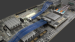
Our work with Samtec on this long-reach demo was covered by Dan Nenni in a SemiWiki post back in 2018. We called the demo “reach beyond the rack”. Below is photo of a unique demo we did at the AI Hardware Summit in 2019. Using Samtec’s ExaMAX Backplane Connector paddle cards and a five-meter ExaMAX Backplane Cable Assembly, we literally ran the “reach beyond the rack” demo between our two booths at the show. I don’t think a demo that spans two booths had ever been done before.

I’ll stop here for now. There will be a lot more interesting information from Samtec over the coming months. Information that will expand your design horizons. In the meantime, you can find out more about Samtec here: https://www.samtec.com.

In closing, I met a lot of very talented folks at Samtec during my time at eSilicon. I’d like to give a shout-out to a couple of them.  I’m sure you’ll be hearing more from these folks. Matt Burns is the technical marketing manager at Samtec. He was interviewed in the SemiWiki story, above. And Ralph Page, system architect at Samtec was the driving force in the design of the five-meter cable demo. He also coined the phrase, “reach beyond the rack”.


Can Threshold Switches Replace Transistors in the Memory Cell?

Can Threshold Switches Replace Transistors in the Memory Cell?
by Fred Chen on 06-08-2020 at 6:00 am

Threshold switch I V

The overwhelming majority of transistors produced in the world are used in memory cells, either as the memory itself (Flash, SRAM), or as the access device (DRAM). Yet, it is not necessary to have a transistor in every memory cell. In 2015, 3D XPoint, the first major product based on transistor-less memory cells, was announced [1]. Crossbar also disclosed details of their own transistor-less memory cell in the same year [2].

What makes transistor replacement attractive?
The driving force behind these developments is the reduction of memory cell footprint. The memory element can be stacked directly on top of a “selector” that acts to pass or block current, depending on the applied voltage across the cell [3]. The selector itself is smaller than a transistor as it is simply a layer stacked between electrodes. The lack of a transistor also removes the restriction to build the memory array directly on top of the silicon substrate, enabling the stacking of multiple layers to form a 3D memory array. Moreover, the circuitry that normally surrounds the memory array can now be placed underneath the array, further saving chip area.

Brief description of threshold switching
Threshold switches have actually been around for a while, in many forms, but gained particular notice after Stanford Ovshinsky published his observations of the switching behavior in disordered semiconductors in 1968 [4]. In particular, phase change memory includes the use of amorphous chalcogenides, which exhibit the following interesting behavior [3,4]:

(1) The amorphous chalcogenide maintains a very high resistance up until a high enough voltage, the threshold voltage (Vth) is reached;

(2) Upon reaching the threshold voltage, the material enters an extremely conductive (“ON”) state, and the voltage across the material is reduced;

(3) The material remains in the conductive state until the voltage across it is reduced below a holding voltage (Vh), which is the voltage needed to sustain a minimum holding current (Ih). At this point, it returns to the initial high-resistance (“OFF”) state.

The behavior can be visualized in an I-V curve below:

Figure 1. I-V curve for a threshold switch. Blue: OFF-to-ON. Red: ON-to-OFF.

A wide variety of materials have been found to support threshold switching [5,6]; furthermore, a number of mechanisms have been found to be consistent with this switching:

  1. Metal-insulator transition [7]
  2. Electrothermal effect [8]
  3. Movement of chemical (ionic) species [5]
  4. Disappearance of small polarons [9]
  5. Order-disorder transition [6]

Regardless of the mechanism(s) involved, the special characteristics of threshold switches, particularly the occurrence of the “snapback”, i.e., the abrupt reduction of voltage after reaching Vth, lead to some important implications for the use of threshold switches.

Threshold switches can only be used with specific resistance-based memories
Threshold switches involve switching between currents orders of magnitude apart. As a result, any memory element connected in series with the threshold switch must also be able to conduct fairly high currents. This precludes the usual charge storage memories like DRAM or Flash which use insulators. Phase change memory is a more common companion to threshold switches [6]. Moreover, some of the other emerging memories may not be compatible either if they will be damaged by the sudden current surge.

Threshold switches need current compliance
Since the current surge in the ON state can be quite dramatic, a current-limiting element in series with the threshold switch is necessary to keep the current within spec. This can be a fixed resistance or an active device like a diode or a transistor. The details of this operation are quite subtle. The voltage on the cell is initially all on the threshold switch in the OFF state. Once it goes on, the voltage on the switch is reduced, so the balance of the voltage must fall on the current-limiting element. The I-V of the current-limiting element determines how much current is passed.

Figure 2. A threshold-switched cell needs a current-limiting element like a resistor to limit the current from reaching damaging levels.

Read current must exceed holding current
In order to stay ON, the threshold switch must continue to pass current larger than the holding current Ih. When the resistive memory element is being read, the threshold switch needs to be ON, so there will be a minimum read current.

The minimum read current also sets a limit on how many times the cell may be read before the memory element is disturbed, i.e., accidentally changed from one resistance state to another. This will be covered again later.

Initiation of threshold switches
Some threshold switches require an initiation (“forming”) step. Equivalently, the threshold voltage drops from its initial value, to which it can eventually recover [10]. The main concern here is whether it drops far enough that the half-selected cell voltage [3] can in fact turn ON the threshold switch.

Voltage margin can be tight
Since threshold-switched memory cells will be arranged in a crosspoint array, operation voltages will be designed accordingly. Figure 3 shows the most commonly used half-select scheme, where unselected cells in the same row or column as the selected cell necessarily receive half the voltage that the selected cell receives.

Figure 3. Crosspoint array bias schemes, enabled by the use of threshold-switched memory cells. Left: half-select scheme. Right: third-select scheme. The circle indicates the selected cell.

In this case, the maximum cell operation voltage is twice the threshold voltage Vth. For a third-select scheme, the unselected cells all receive +/- 1/3 the voltage on the selected cell. Therefore, the maximum operating voltage is 3x the threshold voltage Vth. Note that the read and write cell voltages must fall into the allowed ranges: (Vth, 2Vth) for half-select, (Vth, 3Vth) for third-select. Since the read voltage in the half-select scheme will be over half that of the write voltage, the chance of read disturb is extremely high. Even for the third-select scheme, the read voltage being over 1/3 the write voltage still poses significant risk in large arrays, as the read voltage will practically be close to 40% of the write voltage. To mitigate this, the read pulse should be very short, definitely much shorter than the write pulse.

Bottom line: cost of memories based on threshold-switching

In the end, widespread acceptance of a given memory technology depends on how effectively its cost can be driven down. Threshold switches offer a significant starting point due to their smaller footprint compared to transistors. Moreover, they are free from the usual transistor scaling issues such as short-channel effects and contact resistance dependence on doping [11, 12]. An even bigger plus is the large current density (>10 MA/cm2) that is generally available [3].

The cell size for a 1X nm DRAM is 0.0026 um2 [13], while the cell size for a 3D XPoint memory is 0.00176 um2 [14], indicating the cell size advantage already exists for a threshold-switched cell. A future cell size of 0.02 um x 0.02 um has an equivalent cell density to 100 stacked layers of 0.2 um x 0.2 um 3D NAND Flash cells, the current state-of-the-art for cell density. A larger cell size of 0.04 um x 0.04 um needs 4 stacked layers to achieve the same density. Thus, scaling threshold switches to 10 nm would provide a big boost to their becoming mainstream. That said, it also requires the readiness of the resistance-based memory element attached to the threshold switch, as mentioned above. Therefore, the replacement of transistors in memory cells by threshold switches requires the widespread acceptance of resistance-based memory as an alternative to charge-based memory.

References
[1] https://en.wikipedia.org/wiki/3D_XPoint

[2] https://ieeexplore.ieee.org/document/7104114?denied=

[3] L. Zhang, S. Cosemans, D. J. Wouters, G. Groesneken, M. Jurczak, B. Govoreanu, “One-Selector One-Resistor Cross-Point Array With Threshold Switching Selector,” IEEE Trans. Elec. Dev. 62, 3250 (2015).

[4] S. R. Ovshinsky, “Reversible Electrical Switching Phenomena in Disordered Structures,” Phys. Rev. Lett. 21, 1450 (1968).

[5] Z. Wang, M. Rao, R. Midya, S. Joshi, H. Jiang, P. Lin, W. Song, S. Asapu, Y. Zhuo, C. Li, H. Wu, Q. Xia, J. J. Yang, “Threshold Switching of Ag or Cu in Dielectrics: Materials, Mechanism, and Applications,” Adv. Func. Mat. 28, 1704862 (2018).

[6] P. Noe, A. Verdy, F. d’Acapito, J-B. Dory, M. Bernard, G. Navarro, J-B. Jager, J. Gaudin, J-Y. Raty, “Toward ultimate nonvolatile resistive memories: The mechanism behind ovonic threshold switching revealed,” Sci. Adv. 6:eaay2830, 2020.

[7] A. L. Pergament, G. B. Stefanovich, A. A. Velichko, S. D. Khanin, “Electronic Switching and Metal-Insulator Transitions in Compounds of Transition Metals https://www.researchgate.net/profile/Alex_Pergament/publication/257231373_Electronic_Switching_and_Metal-Insulator_Transitions_in_Compounds_of_Transition_Metals/links/5475ad030cf245eb4370f15e/Electronic-Switching-and-Metal-Insulator-Transitions-in-Compounds-of-Transition-Metals.pdf

[8] J. M. Goodwill, A. A. Sharma, D. Li, J. A. Bain, M. Skowronski, “Electro-Thermal Model of Threshold Switching in TaOx-Based Devices,” ACS Appl. Mater. Interfaces 9, 11704-11710 (2017).

[9] D. Emin, Polarons, Cambridge University Press, 2013, 180-185.

[10] https://thememoryguy.com/nvm-selectors-a-unified-explanation-of-threshold-switching/

[11] A. Razavieh, P. Zeitzoff, D. E. Brown, G. Karve, E. J. Nowak, “Scaling Challenges of FinFET Architecture below 40nm Contacted Gate Pitch,” 75th Annual Device Research Conference, 2017.

[12] https://www.linkedin.com/pulse/contact-resistance-silent-device-scaling-barrier-frederick-chen

[13] https://www.techinsights.com/blog/samsung-18-nm-dram-cell-integration-qpt-and-higher-uniformed-capacitor-high-k-dielectrics

[14] https://www.techinsights.com/blog/intel-3d-xpoint-memory-die-removed-intel-optanetm-pcm-phase-change-memory

Related Lithography Posts


Do You Love DAC? Here’s Why I Do

Do You Love DAC? Here’s Why I Do
by Mike Gianfagna on 06-07-2020 at 10:00 am

I Love DAC Over The Years

Hello all, and welcome to DAC Season. As you all probably know by now, there are some twists to DAC Season this year. First, it’s being held July 20 – 24 this year instead of in June. I believe there was one other time the conference spilled into July, so this isn’t the norm. DAC, like pretty much every other conference these days has also gone virtual. Where to locate DAC has always been the source of a lot of passionate opinion and discussion. This time, we get a pass on that.

The conference chair this year is Dr. Zhuo Li from Cadence. Dr. Li has quite the challenge, presiding over a conference that is doing a lot of things for the first time with respect to both space and time. You can watch his series of video blogs that chronicle the momentum of DAC and the recent decision to make it virtual on DACtv here. They’re quite informative and Dr. Li does have a sense of humor.

I want to talk a bit about the I Love DAC movement – it’s history, motivation and evolution. First, let’s take a look at DAC 2020. The technical program has always been of high quality, with relevant topics and no-nonsense technical content. This year is no exception.

You can check out the keynotes and SKY Talks on the DAC homepage. There’s also a lot of tutorials there. If you want to cruise through the entire conference agenda, you can check out the conference program here. Whether your interests are technically oriented or business motivated, you’ll find things in this agenda you’ll want to see.

The virtual exhibits portion of DAC is taking shape. There will be new content to download, videos to watch, chats with staff from exhibiting companies and the opportunity to schedule private video meetings. Except for the tchotchkes, pretty much everything you would do at the live version with no sore feet at the end of the day and (potentially) no hangover the next morning.

You can register for DAC here. You’ll notice the rates are less expensive than prior years. That’s another benefit of a virtual conference. You’ll see an I Love DAC registration that provides access to the virtual exhibits, daily keynotes, SKY Talks, tech talks, analyst reviews, design-on-cloud presentations, RISC-V presentations and the daily virtual happy hour. The fee is an attractive $0. You can get more details about I Love DAC here. This is a lot of content for free and I want to spend the rest of the post providing some history on I Love DAC and how it evolved to the killer deal offered today. By the way, I believe the virtual happy hour is BYOB. That means break out the good stuff and catch up with colleagues. So, on to a bit of I Love DAC history…

It was April 2009. I was the VP of marketing at Atrenta (the company that brought you SpyGlass). We were brainstorming about ways to increase booth traffic. How do we get more people to DAC? How do we make sure all those suites in our huge booth would be occupied during the show? It was the same every year by the way. Going into the weekend before DAC, our suite appointments would typically be at around 70%. By noon on Monday (the first day of the show), we’d be over 100%. What that means is we started booking the bistro tables in the booth storefront for overflow meetings.

In spite of this track record, we still struggled to figure out how to get more folks to the show and to the Atrenta booth. There was free Monday, which provided a free exhibit pass to attendees directly from DAC. That program had been on and off over the years, but it was only one day and the exhibits were open for four days in 2009. Then, I got a call from David Lin, the VP of marketing at Denali. Those who’ve been going to DAC for a while will remember the epic Denali parties and their ever-popular EDA Idol contest. Denali was the king of DAC after dark, so when David Lin called with an idea you definitely wanted to listen.

David had a really great idea. Exhibitors at DAC had the opportunity to purchase exhibit passes for the entire week. David had also been talking with Scott Sandler at SpringSoft and he proposed that the three of us, Denali, SpringSoft and Atrenta jointly purchase 600 week-long exhibit passes and hand them out on a first-come, first-served basis to current and recently laid off EDA users. I thought this was a brilliant idea, so did Scott Sandler. And so, the I Love DAC movement was born.

I Love DAC was always sponsored by three companies. The original three did it for a while. It was VERY popular. We designed a unique I Love DAC badge each year and that became a collectible item. At Atrenta, we had some fun promoting the event with a video of someone who thought I Love DAC was a dating site. After a few years, the DAC Executive Committee brought I Love DAC into the formal program and it became a DAC institution and continues to today.

So that’s the I Love DAC story. I suspect there are plenty of SemiWiki readers who were around to see this all unfold. My memory isn’t what it used to be, or at least I don’t think so. Anyway, if I left out any important details please feel free to comment. Have fun at DAC this year.


Google Coming to Your Car

Google Coming to Your Car
by Roger C. Lanctot on 06-07-2020 at 6:00 am

Google Coming to Your Car SemiWiki

Casual observers of the automobile industry are quick to compare connected cars to “smartphones on wheels.” It’s a simple way of looking at things that makes some sense now that half of all cars produced in the world are made with a built-in cellular modem…or two. It belies the complexity of connecting cars, but maybe it’s an accurate way to look at things now that Google’s Android operating system is on its way to dominating in-dash infotainment systems.

Strategy Analytics estimates Android’s share of the global smartphone market at 86%. Android is a long way from that kind of dominance in the world of the connected car, but the die is cast. Android is steadily muscling aside Blackberry’s QNX operating system, legacy Microsoft offerings, various Linux distributions, and a handful of other bespoke systems.

Cars are different. Winning the infotainment system OS race is not a zero sum game. Unlike smartphones, cars have multiple operating systems, multiple networks, and multiple microprocessors. Still, Android’s arrival and impending hegemony in the automotive industry has massive implications.

Car makers are attracted to Android because it promises lower development costs. There are many more app developers working in Android, thanks in large part to that smartphone market dominance, which means they are both readily available and less expensive to hire.

Just like those smartphones, though, cars will require frequent software updates – and that’s a trick that is relatively foreign to the average auto maker. Only Tesla Motors has managed to make automotive software updates look easy – and Tesla isn’t even using Android…yet.

Android arrives at a point in time when creating and managing millions of lines of code is beginning to dominate the design process at most auto makers. The emerging and growing mountain of software code is driving massive hiring and pushing auto makers to seek out sources of savings.

In shifting to Android the industry is looking for development savings of 30%-40%, but there’s a catch. Not only will all that “relatively” inexpensive code require updates – it is also likely to demand greater processing power, memory, and storage capacity – in anticipation of dozens of software updates likely to occur over the estimated decade-long life of any given vehicle.

That’s a pretty big fly in the ointment. Under-resourced infotainment systems are a sore point that continues to plague the automotive industry. Cars are being sold and driven today that lack sufficient processing or memory resources to support their Android and, yes, non-Android systems.

In essence, the onset of Android is opening the automotive industry to a veritable ocean of clever code and related applications. It is also contributing to the auto industry’s pivot toward the rapid adoption of over-the-air (OTA) software update technology. That, in turn, is broadening the deployment of cloud-based services and applications including everything from hybrid navigation to digital assistants and edge computing.

It’s also introducing a wider range of failure points, cyber security vulnerabilities, and plain old software bugs. But a properly configured system, equipped with OTA update capability, can enable a car maker to maintain or extend the value of a vehicle or even avoid expensive in-person recalls.

Software-related recalls are a growing challenge for auto makers. An over-the-air software update capability may allow some auto makers to avoid expensive recalls. Recalls are a major inconvenience and, in most cases, a safety threat. Even auto makers hate recalls, which cost $300 per dealer recall visit on average.

Andy Gryc, co-founder of Third Law autotech marketing, was kind enough to compile recall statistics from the National Highway Traffic Safety Administration. Gryc’s recall analysis shows software-related issues have grown in number creating an increased financial exposure for auto makers and driving the adoption of over-the-air (OTA) updating technology.

Third Law recall research: http://www.thirdlawreaction.com/automotive-recalls-infographic-2019/

Multiple suppliers such as Harman International, Wind River, and Aurora Labs have stepped in with OTA solutions as has the eSync Alliance. The 10-member eSync Alliance has rolled out a software developer kits to accelerate the adoption of OTA updates across the industry.

Excelfore OTA announcement: https://excelfore.com/blog/excelfore-esync-sdk-drives-low-cost-low-risk-integration-of-ota/

There’s just one problem. No OTA system, no matter how clever, can make up for insufficient processing capacity or memory. In their rush to pinch pennies, auto makers are putting themselves in a bind.

Google’s Android operating system is a resource hog. Nevertheless, many auto makers are tacking in Google’s direction, adding the Android Auto smartphone mirroring solution. Renault, Volvo, and General Motors are preparing to launch GAS – Google Automotive Services.

It appears that the auto industry is coming to terms with its FOG – Fear of Google. Resistance remains – as some auto makers worry they will lose control of their customers in a whole-hearted embrace of Google – but resistance need not be futile.

Not all auto makers are adopting Android. Tesla is perhaps the most notable exception, but there are many others. Most auto makers are seeking ways to collaborate with Google without surrendering control of their own platforms.

The bottom line is that Android does not travel light. It’s an OS with a lot of baggage. Auto makers can get to their destination, achieve their objectives, without Android. The growing volume of software code, though, calls for providing adequate hardware resources and OTA capabilities.

Cars need OTA update capability for map updates, cyber security patches and updates, and, perhaps most essentially, to add features, functions, and value to cars after the sale. Cars are increasingly defined by software, and cars defined by software will need connectivity and updates. Make sure your next car is connected and updatable. That’s a solid takeaway.


8 Key Tech Trends in a Post-COVID-19 World

8 Key Tech Trends in a Post-COVID-19 World
by Ahmed Banafa on 06-05-2020 at 10:00 am

8 Key Tech Trends in a Post COVID World

COVID-19 has demonstrated the importance of digital readiness, which allows business and people’s life to continue as usual during pandemics. Building the necessary infrastructure to support a digitized world and stay current in the latest technology will be essential for any business or country to remain competitive in a post-COVID-19 world. [3]

COVID19 pandemic is the ultimate catalyst for digital transformation and will greatly accelerate several major trends that were already well underway before the pandemic. The #COVID-19 pandemic will have a lasting effect not only on our economy, but on how we go about our daily lives, and things are not likely to return to pre-pandemic norms. While this pandemic has forced many businesses to reduce or suspend operations, affecting their bottom line, it has helped to accelerate the development of several emerging technologies. This is especially true for innovations that reduce human-to-human contact, automate processes, and increase productivity amid social distancing. [2]

The following technologies stand to bourgeon in a post COVID19 world:

1) Artificial intelligence (AI)
By 2030 #AI products will contribute more than $15.7 trillion to the global economy. A number of technological innovations such as intelligent data processing, and face and speech recognition have become possible due to AI [3]

Post-COVID-19, consumer behaviors won’t go back to pre-pandemic norms. Consumers will purchase more goods and services online, and increasing numbers of people will work remotely. As companies begin to navigate the post-COVID-19 world as economies slowly begin to reopen, the application of artificial intelligence (AI) will be extremely valuable in helping them adapt to these new trends. [2]

AI will be particularly useful for those within retail and supply chain industries. Through machine learning and advanced data analytics, AI will help these companies detect new purchasing patterns and deliver a greater personalized experience to online customers. [2]

AI tools analyze large amounts of data to learn underlying patterns, enabling computer systems to make decisions, predict human behavior, and recognize images and human speech, among many other things. AI-enabled systems also continuously learn and adapt. These capabilities will be extremely valuable as companies confront and adapt to the next normal once this pandemic subsides. [2]

AI will increasingly contribute to the forecasting of consumers’ behavior, which became hardly predictable, and to help businesses organize effective logistics. Chatbots may provide clients’ support 24/7, one of the ‘must-have’ during the lockdown. [3]

2) Cloud computing
Fortunately, #cloud companies are weathering the pandemic stress-test caused by the sudden spike in workloads and waves of new, inexperienced users. Microsoft reports a 775% spike in cloud services demand from COVID-19. [6]

In post-COVID-19 world, cloud technology is likely to receive a surge in implementation across all types of apps. As the virus spread, people were forced to work from home (WFH) and online learning models were implemented, the demand for cloud-based video conferencing and teaching has skyrocketed. Various cloud service vendors have actively upgraded their functions and provided resources to meet this demand. Moving forward, businesses and educational institutions are likely to continue to make use of this technology. As demand for this technology continues to grow, implementation of this technology into mobile applications for easier access will be key, for the cloud the sky is the limit. [2]

3) VR/AR
This pandemic increased the number of people using #VR headsets to play video games, explore virtual travel destinations and partake in online entertainment, as they isolate at home, they’re also using this technology to seek human interaction through social VR platforms.

Businesses have also been experimenting with VR platforms to train employees, hold conferences, collaborate on projects, and connect employees virtually. For example, scientists worldwide have turned to VR platform for molecular design, to collaborate on coronavirus research and potential treatments. Now that businesses and consumers know the extent to which this technology can be used, we are likely to see more virtual conferences and human interactions as our new normal sets in. [2]

4) 5G Networks
5G is acknowledged as the future of communication and the cutting edge for the entire mobile industry. Deployment of #5G networks will emerge between 2020 and 2030, making possible zero-distance connectivity between people and connected machines. This type of mobile internet connectivity will provide us super-fast download and upload speeds (five times faster than 4G capabilities) as well as more stable connections. [3]

The industry buzz surrounding 5G technology and its impact on the next-generation of connectivity and services has been circulating over the last year or so. Yet, the technology still isn’t widely available and it holds the potential to revolutionize the way mobile networks function, because of COVID-19, the 5G market may materialize sooner than expected. As large numbers of people have been forced to isolate, an increase in working and studying from home has been stressing networks and creating higher demand for bandwidth. People have now realized the need for faster data sharing with increased connectivity speeds, an acceleration in the rollout of 5G technology to ensure the bandwidth and capacity challenges of existing infrastructure is more real than ever. [2]

5) Voice User Interface (VUI)
As consumers are becoming increasingly concerned that their mobile devices (which are touched more than 2,600 times per day) can spread #coronavirus. As the fear of spreading germs grows, so will the use of voice tech in forms of voice user interface (VUI) , which can reduce the number of times one touches any surface, including our mobile devices. Almost 80% of our communications done using verbal communication, that’s why voice usage will continue to increase and extend to other smart-home components implicated as major germ hubs. As more TVs and entertainment components, light switches, appliances, plumbing fixtures, and alarm systems incorporate voice control functionality, there will be less need to touch them.

6) Internet of Things (IoT)
IoT will enable us to predict and treat health issues in people even before any symptoms appear, with smart medication containers, IP for every vital part of your body for the doctor to hack. to smart forks that tell us if the food is healthy or not. Personalized approaches concerning prescribing medicines and applying treatments will appear (also referred to as precision medicine). In 2019 there were about 26 billion IoT devices and it’s estimated by statista.com that their number will increase to 30.73 billion in 2020 and to 75.44 billion in 2025. The market value is about $ 150 billion with estimated 15 IoT devices for a person in the US by 2030.

#IoT also fuels edge computing, thus data storage and computation become closer to the points of action, enabling saves in bandwidth and low latency. IoT will transform the user experience profoundly, providing opportunities that weren’t possible before. Gaining this experience may be forced by the pandemic, when people are spending almost all their time at home. IoT devices, that make life quality better and daily life more comfortable can become quite trendy. For example, telemedicine and IoT devices helping to monitor people’s health indicators may increase their popularity.[3]

7) Cybersecurity
Cybersecurity is one of the vital technologies for organizations, especially whose business processes are based on data-driven technologies. Much more attention is being paid to privacy and data protection since the European Union’s General Data Protection Regulations (GDRP) has been signed and recently CCPA in California.

During COVID19 pandemic lock-down, when thousands of people are forced to work remotely, volumes of private data may become totally vulnerable or at least not protected in a proper way. This emerging challenge may give another incentive to the Implementation of #cybersecurity practices. Cybercriminals took advantage of the fear factor of this virus to send their own viruses, there are many examples of such activities recently including fake domains of COVID19, phishing emails promising virus protection kits and even info about canceled summer Olympic games. In addition there is an increase in ransomware attacks on health institutions and even hacking of research centers to steal any info about possible vaccine of COVID19. [3]

8) Blockchain Technology
The COVID-19 crisis has revealed a general lack of connectivity and data exchange built into our global supply chains. Future resiliency will depend on building transparent, inter-operable and connective networks. If there were any lingering doubts over the value of blockchain platforms to improve the transparency of businesses that depend on the seamless integration of disparate networks, COVID-19 has all but wiped them away. We should look at this healthcare crisis as a vital learning curve that can show us how to build transparent, inter-operable and connective networks. #Blockchain is supporting efforts around the globe to battle the virus as explained in the following list [4]:

1)    Tracking Infectious Disease Outbreaks,

2)    Donations Tracking,

3)    Crisis Management and

4)    Securing Medical Supply Chains.

Tracking Infectious Disease Outbreaks

Blockchain can be used for tracking public health data surveillance, particularly for infectious disease outbreaks such as COVID-19. With increased blockchain transparency, it will result in more accurate reporting and efficient responses. Blockchain can help develop treatments swiftly as they would allow for rapid processing of data, thus enabling early detection of symptoms before they spread to the level of epidemics. Additionally, this will enable government agencies to keep track of the virus activity, of patients, suspected new cases, and more. [5]

Donations Tracking
With the help of blockchain capabilities, donors can see where funds are most urgently required and can track their donations until they are provided with a verification that their contributions have been received to the victims. Blockchain would enable transparency for the general public to understand how their donations have been used and its progress. [5]

Crisis Management
Blockchain could also manage crisis situation. It could instantly alert the public about the Coronavirus by global institutes like the World Health Organization (WHO) using smart contracts concept. Not only it can alert, but Blockchain could also enable to provide governments with recommendations about how to contain the virus. It could offer a secure platform where all the concerning authorities such as governments, medical professionals, media, health organizations, media, and others can update each other about the situation and prevent it from worsening further without censorship. [5]

Securing Medical Supply Chains
Blockchain has already proven its success stories as a supply chain management tool in various industries; similarly, Blockchain could also be beneficial in tracking and tracing medical supply chains. Blockchain-based platforms can be useful in reviewing, recording, and tracking of demand, supplies, and logistics of epidemic prevention materials. As supply chains involve multiple parties, the entire process of record and verification is tamper-proof by every party, while also allowing anyone to track the process. [5]

Ahmed Banafa, Author the Books :

Secure and Smart Internet of Things (IoT) Using Blockchain and AI

Blockchain Technology and Applications

Read more articles at : https://medium.com/@banafa

References

[1] https://www.weforum.org/agenda/2020/04/10-technology-trends-coronavirus-covid19-pandemic-robotics-telehealth/

[2] https://clearbridgemobile.com/five-emerging-mobile-trends-in-a-post-covid-19-world/

[3] https://www.sharpminds.com/news-entry/the-future-of-it-covid-19-reality-5-technology-trends/

[4] https://www.weforum.org/agenda/2020/05/why-covid-19-makes-a-compelling-case-for-wider-integration-of-blockchain/

[5] https://medium.com/datadriveninvestor/blockchain-technology-and-covid-19-c504fdc775ba

[6] https://www.zdnet.com/article/microsoft-cloud-services-demand-up-775-percent-prioritization-rules-in-place-due-to-covid-19/


Webinar: Hyperscale SoC Validation with Cloud-based Hardware Simulation Framework

Webinar: Hyperscale SoC Validation with Cloud-based Hardware Simulation Framework
by Daniel Nenni on 06-05-2020 at 6:00 am

Slide1

S2C has been developing FPGA prototyping platforms since 2003, and, over time, their FPGA prototyping platforms have supported increasingly larger more sophisticated FPGA prototyping projects with three key attributes; 1) scalable prototyping gate capacities, 2) a high-speed interface between the FPGA prototype and software running on a host computer, and 3) support for globally distributed users.  A natural evolution of these three FPGA prototyping attributes has led S2C to produce its latest FPGA prototyping platform dubbed the “Prodigy Cloud System”.

WEBINAR REGISTRATION

Hyperscale SoC Validation Gate Capacity – Driven by customer demand for what S2C calls “Hyperscale SoC Validation”, S2C’s Prodigy Cloud System now supports very large SoC prototyping requirements up to 2 billion gates (“Hyper”) in a modularly scalable way … hence “Hyperscale”.  To achieve Hyperscale capabilities, S2C has harnessed the latest and largest Intel FPGA called the Stratix 10 GX 10M FPGA.  This Intel FPGA blows away all other FPGAs generally available today with an estimated usable gate capacity of 80M gates per FPGA.  The GX 10M FPGA is fabricated with Intel’s 14nm silicon, so its expected to run faster and consume less power.  Intel acknowledges in its GX 10M FPGA press release1 that “One market in particular has a critical interest in always using the largest available FPGAs: the ASIC prototyping and emulation market.”  Intel sees FPGA emulation and prototyping supporting a variety of system development tasks including;

  • Algorithm development using real hardware
  • Early SoC software development prior to the chip’s manufacture
  • RTOS verification
  • Corner-case condition testing for both hardware and software
  • Regression testing on successive design iterations

The S2C Prodigy Cloud System comes in a standard server rack and can scale up to eight (8) Quad 10M Logic Systems, each with four (4) GX 10M FPGAs, so one server rack can house up to 32 GX 10M FPGAs.  With an estimated 80 million gates per FPGA, the Prodigy Cloud System should easily support 2 billion gates for FPGA prototyping!  And, if that’s not enough gate capacity, multiple server racks can be connected together.

Fast Interface to Simulation Environment – The second key attribute of the Prodigy Cloud System is an out-of-the-box hardware and software solution for applying large quantities of real-world test data in the form of bus traffic, communications traffic, video images, etc. to the FPGA prototype from your host computer.  This approach creates what S2C calls a “simulation infrastructure” that enables the user to connect the SoC hardware model in the FPGA to a simulation-like verification environment on the host computer.

S2C calls this option ProtoBridge, and it includes PCIe bridge and AXI master/slave logic that is compiled and downloaded into the FPGA together with the SoC prototype design.  The host computer connects to the FPGA prototype with a PCI cable that supports up to 1GB/s transfers, and ProtoBridge includes PCI driver software, and a set of C-API function calls to drive AXI bus transactions from the host computer.Global Remote Access and Control – The third key attribute of the Prodigy Cloud System is support for multiple globally distributed users.  Large SoC design teams today may be spread across multiple locations in the US, Europe, China, India, and Vietnam, so remote access to the FPGA prototyping resources is essential for an optimal ROI from the prototyping investment.

To address this key attribute, S2C has developed what it calls Prodigy Neuro hardware and software.  The Prodigy Neuro hardware, called the Prodigy Neuro Control Module, manages global power control to the FPGA hardware, clocks and resets, self-test, and monitoring of the Prodigy Cloud System FPGA board connections.

Prodigy Neuro Software provides centralized control of the Prodigy Cloud System hardware resources, as well as user and prototyping project management.  Prodigy Neuro Software includes a browser-based GUI for easy remote access to Prodigy Cloud System hardware for centralized resource control and multi-design management and monitoring.  Prodigy Cloud System hardware can be allocated to multiple different projects running simultaneously on the hardware, with 3-level permission control for multiple users.  Prodigy Neuro Software also provides FPGA prototyping hardware usage analytics, warnings of hardware faults, and auto-detection of hardware connection with instant messaging upon first check-in.So, if you thought that your SoC designs were too large for FPGA prototyping, or you needed a shareable FPGA prototyping resource for a globally distributed design team and multiple FPGA prototyping projects, you should register for this webinar. You will get a copy of the replay if you can’t attend the live broadcast.

WEBINAR REGISTRATION

Also Read:

WEBINAR: Prototyping With Intel’s New 80M Gate FPGA

S2C Delivers FPGA Prototyping Solutions with the Industry’s Highest Capacity FPGA from Intel!

AI Chip Prototyping Plan


Automating the Analysis of Power MOSFET Designs

Automating the Analysis of Power MOSFET Designs
by Daniel Payne on 06-04-2020 at 10:00 am

ventilator

There’s a world of difference between our smart phones that are battery powered and pack billions of transistors, and power MOSFET devices that can be used in industrial applications, telecom, cloud computing and automotive where they could be run at a few hundred volts and up to 80A of current. I’ve read about one power MOSFET company called Monolithic Power Systems, Inc. (MPS) because they were in the news recently with an open-source ventilator to help out during the COVID-19 pandemic. Now that’s a noble goal to have.

MPS Open-Source Ventilator

MPS also uses some EDA tools to help automate their IC design process of power MOSFET devices, and back in June 2019 they talked about using Polas from Empyrean. I followed up on WebEx with Kyle Tsai at Empyrean to see what Polas had to offer, and then better understand the design challenges.

Designers of power MOSFET devices have a handful of challenges, like:

  • Reaching a low Rds value to meet spec
  • Sufficient metal interconnections
  • Package and pad locations that work
  • Vias and contacts that allow large, peak currents
  • Meeting dead-time specs

Shown below is a schematic with two MOSFET devices, the one on top is called high-side, and the one on the bottom is called low-side. The gates of each MOSFET are pulsed at complimentary times:

MOSFET timing, schematic

Simplified MOSFET layout

The four types of analysis that the Polas tool offers for power MOSFET devices include:

  1. Rdson
  2. EM/IR drop
  3. Timing Delay
  4. Cross-talk

IC layout creates parasitic RC values, and these most be accounted for during each analysis because they impact how the device performs in trying to meet all of the specifications. Polas uses some clever technology to account for IC layout and parasitics:

  • A field solver to account for irregular polygons
  • Split MOS for the most accurate interconnect resistance
  • Fast-mode Rds(on) and IR drop analysis without dynamic circuit simulation
  • SPICE-based simulation mode for Rds(on) and IR drop analysis

In just a few minutes you can get a very detailed report of Rdson effective resistance with Polas:

Rdson Effective Resistance

EM/IR drop analysis uses a color gradient (red – large drop, blue – small drop) to show the weak and strong spots of your layout, so the design engineer can communicate to the layout designer on which areas need to have wider metal or improved vias and contacts:

EM IR drop analysis

Timing delay analysis uses a circuit simulator called ALPS, and colors show how the delay changes across the IC layout view:

Timing Delay Analysis by Circuit Simulation

Cross-talk is the capacitive coupling of adjacent IC layers, so the analysis shows the engineering team all of the coupling nets and their capacitive coupling so that better layout decisions can be made to minimize the effect. Here you can see the cross-probing between the coupling list reported on the left, with the layout on the right:

Cross-probe of Coupling Capacitance

Setting up and using Polas is straight forward, you’ll just need the PDK files from your foundry and the IC layout, so it fits nicely into your design flow. Some other unique features with Polas are support of:

  • Tandem MOS devices
  • Different widths and types in the layout
  • Pre-drivers for power MOS

Supported Features

Customer Case 1

A Polas user doing charger power MOS designs with a BCD technology and they needed to do pad location analysis and optimization. With this tool they were able to calculate the Rdson values and current density. Next, they optimized the pad number and location, meeting cost and performance goals. Here’s a table showing their Pad number, Rdson value, top metal resistance and the maximum current densities:

Customer Case 2

In this scenario engineers were designed a vehicle power MOS on a BCD process, and they ran the timing analysis to help optimize their layout to meet timing specifications. The good news is that it took only one pass of silicon to get their results. Notice that this layout uses 12,000 fingers.

Vehicle – Power MOS, BCD Process

Summary

Industrial, telecom, cloud computing and automotive designs are all using power MOSFET chips, and with their unique environments come challenging design requirements. It’s now possible to use EDA tools like Polas from Empyrean to quickly and accurately analyze Rdson, EM/IR drop, timing delays and cross-talk effects.

Related Blogs


Webinar Replay – Insight into Creating a Common Testbench

Webinar Replay – Insight into Creating a Common Testbench
by Tom Simon on 06-04-2020 at 6:00 am

Common Tesbanch

These days the verification process starts right when the design process begins, and it keeps going well past the end of the design phase. Simulation is used extensively at every stage of design and can go a long way to help validate a design. However, for many types of designs, especially those that process complex data streams, emulation has to be used to ensure proper operation. In a recent webinar Aldec not only discusses the limitations of simulation-only verification for ASICs and large FPGAs, they also help show how it is possible to create common testbenches that are applicable to emulation as well to improve efficiency and help in problem diagnosis.

In the webinar titled Common Testbench Development for Simulation and Prototyping, Alexander Gnusin goes into great detail about the reasons for using a common testbench between simulation and emulation, and then he dives into the specifics of how to make it happen.

Given the relatively slow speed of simulation, emulation is the only way to run enough cycles to ensure that large designs operate properly with large frame sizes. Similarly, simulation time increases as more of the system is included in the scope. Real hardware environments also differ from simulations, so it is important to factor this in as well. Lastly, as reliable as synthesis and STA are, it is imperative to simulate at the gate level to ensure the hardware implementation is correct.

Yet, there are a number of issues that must be dealt with to enable emulation. It is necessary to deal with fundamental issues, such as the cycle based I/O in hardware designs. Cycle based I/O stimulus can overload emulator interfaces. Alexander discusses eliminating this issue by adding extra code in the hardware domain to eliminate the need for cycle based communication. Also, he mentions lowering the overall transaction frequency. Alexander talks about adding synthesizable verification components, such as drivers, monitors, responders and checkers.

The webinar takes time to discuss how common test benches should be set up. Alexander goes through the coding steps using Aldec’s HES DVM, which is a hybrid verification platform. Aldec uses SCE-MI for function based transaction level co-emulation technology. The common testbench will have two top levels – an HDL top and an HVL top. The HVL level uses SystemVerilog and optionally UVM. The HDL level uses SystemVerilog RTL with extra SCE-MI2 compiler features.

There are some helpful coding enhancements for emulation available from SCE-MI2 compiler features. Among these are implicit state machines, use of shared registers, clock and reset generation templates, use of hierarchical read access, writing and reading of MEM arrays and File I/O. The webinar provides examples of each of these to help better understand what is offered.

Alexander covers some useful techniques that can improve common testbench effectiveness. The LFSR-based seed-programmable randomization techniques can reduce connection load and provide useful stimulus. Also, He suggests using synthesizable FIFO-based scoreboards for datapath checking. To verify the equivalence of packets or data chunks, Alexander suggests compressing them to short signature using CRC or FCS methods and perform the datapath checking just on those signatures. End of test statistical verification can be based on the comparison of configurable counters values in the design and verification components.

Aldec’s HES DVM allows for optimization to improve speed though several methods that Alexander discusses in the webinar. Once the common testbench has been assembled Aldec’s Riveria Profiler can provide estimates of the maximum emulation speed up.

There is not space here to go through the whole process, but the remainder of the webinar lays out the common testbench development process and then goes through a design example. This detailed and informative webinar is available for replay on the Aldec website.


Tesla Driving on the Edge

Tesla Driving on the Edge
by Roger C. Lanctot on 06-03-2020 at 10:00 am

Tesla Driving on the Edge

It’s happened again. Yesterday, on a highway in Taiwan, a Tesla Model 3 plowed into the trailer of an overturned truck. Accounts of the event suggest the vehicle’s Autopilot system was engaged. The failure of the system to perceive the danger ahead and avoid the inevitable collision suggests an “edge case” scenario – wherein the Autopilot system encounters a circumstance that has not previously been encountered or anticipated in its algorithms.

The video is HERE.

The expression “edge case,” like collateral damage, is a euphemistic way of describing a potentially life-threatening driving situation. Usually, edge cases are unfamiliar objects in the roadway or familiar events that are difficult for on-board computers to interpret due to environmental interference such as lighting, weather, or occlusion from other vehicles.

The crash in Taiwan is reminiscent of multiple previous Tesla Autopilot-engaged crashes that have included driving under trailers and driving into emergency responder vehicles parked in travel lanes. The crash in Taiwan is notable for several reasons including:

  • The Tesla Model 3 completely fails to perceive that the lane in which it is driving is completely blocked by the overturned truck in its path.
  • The Tesla Model 3 completely fails to perceive the truck driver (visible in the video) who has walked forward against the direction of traffic in order to warn oncoming cars away from his overturned vehicle. The truck driver is clearly shown dodging the oncoming Tesla.
  • It is possible that the shrubbery mounted atop the highway barrier on the left side of the lane has interfered with the Model 3’s radar – causing the perception failure.
  • Bright sunlight, coming from the driver’s left, does not appear to be a factor – or should not have been a factor.

Who should be worried?

  • Tesla owners with Autopilot activated should be concerned. It is not at all clear that this is an easily corrected weakness in Autopilot.
  • Regulators should be concerned, as this may or may not be a flaw in Autopilot’s ability to protect drivers. It may require action.
  • General Motors, Toyota, Audi, Nissan, et.al. Multiple competing car makers are developing or have already launched their own Autopilot equivalents – such as GM’s Super Cruise – offering “supervised” automated driving. As these companies ponder stepping up to un=supervised Level IV operation, they will do well to take into account the performance of Tesla Autopilot in this circumstance.

What can be done?

This latest Tesla crash highlights the importance of vehicle-to-cloud/infrastructure connectivity. The existence of traffic camera video to capture the event in question thereby facilitating forensic assessment of the event implies the ability of traffic monitoring authorities to use existing video to warn drivers of dangerous traffic conditions in real time.

Companies such as Savari Network, Haas Alert, Notraffic, and TrafficLand are all working on leveraging wireless connections and traffic camera and other resources to alert drivers to danger ahead. It is not clear from the video how much time has transpired from the truck crash to the Tesla crash, but there was enough time for the truck driver to exit his vehicle and walk down the road to warn oncoming drivers. That ought to have allowed enough time for traffic monitoring systems or personnel to have sent either an automated or manual alert to all drivers headed toward the event.

Those alerts or warnings could have been delivered via telematics service providers, smartphone apps, or embedded vehicle systems with in-dash navigation. The bottom line, existing cellular and camera-based highway monitoring systems could have been used to help avoid the unfortunate demise of yet another Tesla operating on Autopilot. The technology exists to solve these kinds of problems today.


Free Webinar on Verifying On-Chip ESD Protection

Free Webinar on Verifying On-Chip ESD Protection
by Tom Simon on 06-03-2020 at 6:00 am

Promo Ad 400x400 1

Walking across a carpet can generate up to 35,000 volts of static charge, which is tens of thousands of times higher than the operating voltages of most integrated circuits. When charge build up from static electricity is exposed to the pins of an IC, the electrostatic discharge (ESD) protection network on the chip is intended to harmlessly shunt the current to ground. Decades of design experience have taught us how to design these protections. However, if the ESD protections are not properly implemented on chip, or if there is a design flaw, such as incorrect design parameters, a chip can fail in the field. ESD related failures can be instantaneous when they are caused by things like a device burnout, or they can be slow when they are caused, for instance, by electromigration (EM).

An ESD failure in the field can be expensive and can even lead to safety issues, depending on the end product application. The best way to ensure that ESD protections, as implemented, are going to prove effective is to verify them in layout prior to tape out. Waiting until testing can waste time and money, and lead to difficulties in identifying the root cause of the problem. Fortunately, there is a way for IC designers to verify the ESD protections on a chip once the layout is available.

Magwel offers its ESD protection network verification tool ESDi to rapidly detect a wide range of design and implementation issues that can lead to ESD failures. ESDi can check for unprotected pins, missing vias, missing or undersized ESD devices, high bus resistance and more. It also uses parallel processing to quickly simulate HBM events on all or a subset of the pin pairs on a chip. The simulation uses TLP models and can accurately model snap back behavior. It can also predict competitive triggering of multiple ESD devices in a single ESD event. ESDi will report current density and EM violations.

Error and violation review is made easy with an advanced user interface for filtering, sorting and selecting errors to view in detail and visualize their locations. False or missed errors are dramatically reduced by using simulation for all tests, instead of having the user pick and choose what potential issues need simulation.

To give a firsthand look at how ESDi is set up and used, Magwel is offering a free webinar on Tuesday June 9th at 10AM Pacific Time. In this webinar Magwel Application Engineer Allan Laser will provide an overview of the tool’s features followed by running a sample design so viewers can better understand each step of operation.

ESDi can be used at the block or chip level. It has its own simulator specifically optimized for ESD event modeling and also has a high accuracy solver-based extractor for use on the design layout. ESDi also has automated and simplified the process of ESD device identification.

ESDi is remarkably effective because its development was based on customer input. The webinar will provide a glimpse into the many large and small features in the tool that make it the choice for many leading semiconductor companies. Registration for the webinar replay of Magwel’s ESDi is available here.

About Magwel
Magwel® offers 3D field solver and simulation based analysis and design solutions for digital, analog/mixed-signal, power management, automotive, and RF semiconductors. Magwel software products address power device design with Rdson extraction and electro-migration analysis, ESD protection network simulation/analysis, latch-up analysis and power distribution network integrity with EMIR and thermal analysis. Leading semiconductor vendors use Magwel’s tools to improve productivity, avoid redesign, respins and field failures. Magwel is privately held and is headquartered in Leuven, Belgium. Further information on Magwel can be found at www.magwel.com