You are currently viewing SemiWiki as a guest which gives you limited access to the site. To view blog comments and experience other SemiWiki features you must be a registered member. Registration is fast, simple, and absolutely free so please, join our community today!
In the early 2000s, Moore’s Law—the observation that the number of transistors on a chip doubles roughly every two years—was facing an existential crisis. As semiconductor nodes shrank below 90nm, planar transistors suffered from debilitating issues: leakage currents soared, power efficiency plummeted, and scaling became unsustainable. Enter Dr. Chenming Hu, widely regarded as the “Father of FinFETs,” whose invention of the Fin Field-Effect Transistor revolutionized semiconductor design and breathed new life into Moore’s Law, enabling the modern era of computing.
Moore’s Law, coined by Gordon Moore in 1965, had driven decades of exponential growth in computing power, fueling everything from PCs to smartphones. By the late 1990s, however, planar MOSFETs (Metal-Oxide-Semiconductor Field-Effect Transistors) hit physical limits. At smaller nodes, short-channel effects caused electrons to leak, increasing power consumption and heat. By 2003, leakage power in 90nm chips was nearly equaling dynamic power, threatening performance and battery life. Scaling transistors further seemed impossible without sacrificing reliability or efficiency, prompting industry leaders to declare Moore’s Law “dead.”
Dr. Hu, a professor at UC Berkeley and a veteran of semiconductor research, proposed a radical solution: the FinFET. Unlike planar transistors, which lie flat on the silicon surface, FinFETs are three-dimensional structures with a thin, fin-like channel protruding vertically. This “fin” is surrounded by a gate on three sides, providing superior electrostatic control over the channel. Introduced in a seminal 1999 paper, Hu’s FinFET design reduced leakage current by orders of magnitude, improved switching efficiency, and enabled scaling to sub-20nm nodes. His team’s simulations showed that FinFETs could operate at lower voltages while maintaining high performance, a critical breakthrough for power-constrained devices.
The impact was profound. By 2011, Intel adopted FinFETs for its 22nm Ivy Bridge processors, marking the technology’s commercial debut. TSMC and Samsung followed, integrating FinFETs into 16nm and 14nm nodes by 2014. FinFETs allowed chipmakers to pack more transistors into smaller areas without the catastrophic leakage of planar designs. For example, Intel’s 22nm FinFET process achieved a 37% performance boost at the same power or a 50% power reduction at the same performance compared to 32nm planar chips. This revitalized Moore’s Law, enabling the development of power-efficient CPUs, GPUs, and AI accelerators.
Hu’s innovation wasn’t just technical; it was a paradigm shift. FinFETs required rethinking transistor architecture, fabrication processes, and design tools. The 3D structure demanded precise lithography and new materials, like high-k dielectrics, to manage capacitance. TSMC’s 7nm FinFET node, powering chips like Apple’s A12 Bionic, achieved transistor densities of over 90 million per mm², a feat unimaginable with planar technology. By 2025, FinFETs remain the backbone of advanced nodes, with TSMC’s 3nm process pushing densities to 200 million transistors per mm², driving AI, 5G, and HPC applications.
Beyond technical merits, Hu’s work had economic and societal impacts. FinFETs extended the viability of Moore’s Law, sustaining the semiconductor industry’s growth. The global chip market, valued at $600 billion in 2024, owes much to FinFETs’ ability to meet demands for faster, smaller, and greener devices. From smartphones to data centers, FinFETs underpin modern technology, enabling AI models like those powering chatbots and autonomous vehicles. Hu’s contributions earned him the 2016 IEEE Medal of Honor and recognition as a visionary who “saved” Moore’s Law.
Challenges remain as scaling approaches 1nm. Quantum tunneling and heat dissipation threaten further miniaturization, prompting exploration of gate-all-around (GAA) transistors and 2D materials. Yet, FinFETs laid the foundation for these innovations, proving that architectural ingenuity could overcome physical limits. Dr. Hu’s legacy is not just in sustaining Moore’s Law but in inspiring a generation of engineers to rethink the impossible. As semiconductors evolve, his FinFET remains a cornerstone, ensuring Moore’s Law endures for years to come.
How do you control your smart TV? With a remote control of course, already quite capable since it allows voice commands to find a movie or TV show without needing all that fiddly button-based control and lookup. But there’s a range of things you can’t do that we take for granted on a tablet or phone screen. Point and click on an object, drag and drop, swipe, or draw freehand (maybe circle an actor to ID). This is what the emerging generation of smart automation for remotes will make possible for TVs, for gaming and for other applications such as interacting with images cast from a PC to a large monitor. LG Smart TVs with Magic Remote have already proven the appeal of an earlier generation of pointing control as LG has included this technology in its flagship and main line Smart TVs since 2010 and over 600 OEMs have licensed their underlying WebOS® providing pointing control enabled by Ceva’s MotionEngine™ sensor fusion software. Now Ceva has extended MotionEngine further, to bring true remote touchscreen-like possibilities to how we can interact with home entertainment and commercial presentation devices.
The opportunity
The global market for smart TVs alone was around a quarter of a trillion dollars in 2023/2024 and is expected to show a CAGR of between 11.5% and 12.8% through 2033. This is closing fast on and may ultimately surpass smart phone market sizes. I guess in a busy, always-on world we still need our passive entertainment down time at the end of the day, much though we like our phones.
Better ways to interact with home (and office) applications have always spurred innovation, as seen in the wide popularity of voice control. Looking for further innovation or parity, TV makers will need to encourage interaction in ways that mirror modern paradigms for touchscreens, without needing to touch the screen. Why not point and drag or wave controls off-screen with your remote? Or shake the remote or draw a symbol on the screen to prompt a user-selected action (jump to your favorite news channel perhaps). I expect that once a trend becomes apparent here it will quickly turn into a flood.
Behind a touchless touchscreen
These systems depend on capabilities in both the host (say a TV) and the remote. The remote uses sensors, such as an inertial measurement unit (IMU), fusing that information to determine pointing position on the target and communicating to the host side software.
Historically these systems have used 3DoF (3 degrees of freedom: pitch, yaw and roll) to sense where the remote is pointing, but more is possible with 6DoF systems combining a 3-axis accelerometer, 3-axis gyroscope and UWB-based position sensing. These can determine position and orientation determination with high spatial and temporal accuracy.
The Ceva-MotionEngine Hex software supports this capability with some unique advantages. First, as a software-only library it is designed to allow OEMs to build around their preferred processor and sensor choices. It also provides absolute cursor positioning, essential to support interactions like precise point and click sensitivity, on- and off-screen gestures and drag and drop.
Further, the library provides the must-have features essential in any application of this nature. Whatever sensors you may be using, Ceva-MotionEngine Hex handles automatic bias calibration, correcting for drift without need for manual calibration. For a hand-held remote, small tremors in holding the remote or pressing buttons could be damaging to accuracy. The library stabilizes against such movements. It supports superior slow-motion detection to select small targets. And it offers very low latency to ensure naturally responsive behavior.
Unsurprisingly given Ceva’s strength in low power applications, the embedded library is designed for systems with very constrained resources and can operate efficiently on low power MCUs or DSPs, just what you need for a TV or gaming remote or a stylus pen designed to write over a PC or projected presentation. It can also reside in the TV operating system (Android®, Linux®, webOS®) simplifying deployment across many platforms and enabling additional advanced features.
The Ceva-MotionEngine Hex advantage
This software library is built on more than two decades of experience working with MEMS IMUs and partners building motion-aware systems. Among these LG Electronics built the library into their Smart TV and Magic Remote back in 2010 and adoption has grown across LG branded Smart TVs and many third-party brand partners since then.
It might seem that at first glance that an OEM might choose to build this capability themselves. According to Chad Lucien (VP and GM for the sensor and audio business unit at Ceva) this isn’t as easy as it might appear. Delivering a production solution is much more complex, including challenges like robustly handling sensor drift over time, understanding the many possible user experiences that could be modeled, and mitigating the impact of users’ hand tremors which can result in large pointing inaccuracies if not addressed.
Translating from a prototype to a robust production solution is where the promise of a remote touchscreen-like experience could fall apart, unless you work with a supplier which has significant and proven experience in this field. To learn more, check HERE.
In a significant milestone for the semiconductor industry, Teradyne was honored as the 2025 TSMC Open Innovation Platform® Partner of the Year for TSMC 3DFabric® Testing. This award, announced on September 25, 2025, underscores the deep collaboration between Teradyne, a leader in automated test equipment and robotics, and TSMC, the world’s premier semiconductor foundry. The recognition highlights their joint efforts in advancing multi-die test methodologies for chiplets and TSMC’s CoWoS® advanced packaging technology, marking a pivotal step in the shift toward chiplet-based architectures essential for AI and high-performance computing.
Teradyne, headquartered in North Reading, Massachusetts, specializes in designing and manufacturing automated test solutions for semiconductors, electronics, and robotics systems. Its portfolio ensures high-quality performance across complex devices, from wafer-level testing to final assembly. TSMC dominates the foundry market with cutting-edge process nodes and packaging innovations. The partnership traces back to at least 1999, when TSMC adopted Teradyne’s automatic test equipment for 0.18-micron test chips. Over the years, this alliance has evolved, with Teradyne contributing to TSMC’s ecosystem through innovations in test strategies for heterogeneous integration.
At the heart of this award is TSMC’s OIP, launched in 2008 to foster collaboration among design partners, IP providers, and ecosystem members. OIP accelerates innovation by integrating process technology, EDA tools, and IP, enabling faster implementation of advanced designs. Celebrating its 15th anniversary in 2023, OIP has grown from 65nm nodes onward, addressing rising design complexities. Within this framework, the 3DFabric Alliance, introduced in 2023, focuses on overcoming challenges in 3D integration and advanced packaging.
TSMC 3DFabric® represents a comprehensive suite of 3D silicon stacking and advanced packaging technologies, encompassing both 2.5D and 3D architectures like CoWoS and InFO. These enable heterogeneous integration, boosting system-level performance, power efficiency, and form factors for applications in AI accelerators, 5G, and HPC. CoWoS, in particular, supports multi-die packages by stacking chips on silicon interposers, ideal for demanding AI workloads.
Through the 3DFabric Alliance, Teradyne and TSMC have pioneered test methodologies that enhance silicon bring-up efficiency and test quality. Teradyne’s investments in UCIe, GPIO, and streaming scan test solutions facilitate scalable, high-quality testing of die-to-die interfaces. UCIe, an open standard for chiplet interconnects, ensures seamless data transfer between dies, while streaming scan enables high-speed testing over these interfaces at wafer sort or probing stages. This reduces defect escapes, lowers quality costs, and accelerates time-to-market for 3D ICs used in AI and cloud datacenters.
Shannon Poulin, President of Teradyne’s Semiconductor Test Group, emphasized the value of TSMC’s collaborative ecosystem: “At Teradyne, we strongly believe in the open and collaborative ecosystem approach of TSMC’s Open Innovation Platform and look forward to continuing our partnership to drive innovation and deliver exceptional value to our customers.” Aveek Sarkar, Director of TSMC’s Ecosystem and Alliance Management Division, congratulated Teradyne, noting their contributions to improving silicon bring-up and enabling AI proliferation through energy-efficient compute.
The award was unveiled at the 2025 TSMC North America OIP Ecosystem Forum in Santa Clara, California, on September 24, 2025. This event gathered industry leaders to explore AI’s role in next-generation designs for TSMC’s advanced nodes like A16, N2, and N3. Highlights included discussions on AI-accelerated chip design, multi-die systems, and 3DFabric advancements, with partners showcasing tools for HPC and energy efficiency.
This partnership not only strengthens Teradyne’s position in AI hardware testing but also propels the industry toward more efficient, scalable semiconductor solutions. As demand for AI and cloud infrastructure surges, collaborations like this will be crucial in shortening development cycles and enhancing reliability. Looking ahead, Teradyne and TSMC’s ongoing innovations promise to redefine heterogeneous integration, driving the next wave of technological breakthroughs
In the fast-evolving semiconductor landscape, electrostatic discharge (ESD) protection is pivotal for ensuring chip reliability amid shrinking nodes and extreme applications. Sofics, a Belgian IP provider specializing in ESD solutions for ICs, has cemented its leadership through strategic collaborations showcased at TSMC’s 2025 Open Innovation Platform Ecosystem Forum. By delivering Power-Performance-Area optimized ESD IP across TSMC nodes from 250nm to 2nm, Sofics enables innovations in AI infrastructure and harsh-environment electronics.
A prime example is Sofics’ partnership with Celestial AI, tackling AI’s “memory wall” bottleneck. As AI models explode in size—410x every two years for Transformers—compute FLOPS have scaled 60,000x over 20 years, but DRAM bandwidth lags at 100x and interconnects at 30x, wasting cycles on data movement. Celestial AI’s Photonic Fabric™ revolutionizes this with optical interconnects, delivering data directly to compute points for superior bandwidth density, low latency, and efficiency. Traditional optics demand DSPs and re-timers, inflating power and latency, but Photonic Fabric uses linear-drive optics, eliminating DSPs via high-SNR modulators and grating couplers.
Sofics customized ESD IP for TSMC’s 5nm process, proven in production, to protect Photonic Fabric’s sensitive interfaces. Tx/Rx circuits operate at ~1V with <20fF parasitic capacitance for 50-100Gbps signals, ensuring signal integrity while fitting dense packaging. ESD ratings hit 50V CDM with <100nA leakage, supporting thin-oxide circuits without GPIO cells. Power clamps handle non-standard voltages (1.2V-3.3V) in small areas, vital for EIC-PIC integration. This collaboration, highlighted at OIP, breaks bandwidth barriers, enabling multi-rack AI scaling. Celestial AI’s August 2025 Photonic Fabric Module, a TSMC 5nm MCM with PCIe 6/CXL 3.1, exemplifies this, backed by $255M funding.
Equally groundbreaking is Sofics’ alliance with Magics Technologies, enabling radiation-hardened (rad-hard) ICs for nuclear, space, aerospace, and medical sectors. Demand surges for rad-hard electronics amid space exploration and nuclear fusion research like ITER, where ICs must endure >1MGy TID and >62.5 MeV·cm²/mg SEE without malfunction. Magics, a Belgian firm with 10+ years in rad-hard-by-design, offers chips like wideband PLLs (1MHz-3GHz, -99dBc/Hz phase noise) and series for motion, imaging, time, power, and AI processing.
Sofics provides rad-hard ESD clamps for Magics’ TSMC CMOS designs, supporting voltages like 1.2V/3.3V with >2kV HBM, <20nA leakage, and <1700um² area. Key features include cold-spare interfaces (latch-up immune, SEE-insensitive up to 80MeV·cm²/mg) and stacked thin-oxide devices for 1.2V GPIOs on 28nm, bypassing thick-oxide limitations. This 15-year TSMC-Sofics tie, via IP & DCA Alliances, ensures early access and quality. Magics’ €5.7M funding in April 2025 accelerates commercialization.
Bottom line: These partnerships underscore TSMC’s ecosystem strength, with Sofics supporting 90+ customers in AI/datacenters (40+ projects) and space (e.g., Mars rover, CERN). By optimizing ESD for photonics and rad-hard apps, Sofics drives innovation, from hyperscale AI to fusion reactors, proving ESD IP’s role in overcoming physical limits.
This article claims to provide clear key insights of Min Pulse Width (MPW) timing signoff check, proactive closure strategies for faster time-to-market, and effective methods to prevent silicon failures.
Min Pulse Width (MPW) check for timing signoff has become an important design constraint at the sub-5nm technology node. Recently, there have been reports from multiple companies of silicon failures associated with MPW. These failures point to inadequate modeling of design margins related to MPW, gaps in timing signoff verification process and underestimation of the issue’s importance. It is essential to recognize and address this challenge to prevent delays in bringing products to market and avoid costly silicon failures.
These issues indicate limited modeling of design margins related to MPW, gaps in the timing signoff verification process, and an underestimation of the significance of the issue.
Min Pulse Width (MPW) for a logical cell is shortest, non-zero finite duration of a logic “high” or “low” signal at the input that can be correctly propagated and processed by the gate at its output as a valid logical transition. MPW requirement acts as low pass filter for rejection of unwanted glitch and transient noise by effectively filtering them.
Impact of MPW Failure
If the input stimulus is narrower than MPW specification, it might be filtered out entirely (absorbed, no change at the output) or attenuated below threshold producing an invalid transition at the output (glitch or runt pulse), leading to logic errors and incorrect circuit behavior besides damaging internal gate circuits due to stress. Also possible at the output is an unstable “metastable state” that can persist for an indeterminate amount of time leading to delays and potential circuit failure.
Relevance to STA Signoff
Transistor symmetry mismatches within gate are increasingly significant at sub 5nm
Crosstalk and wire induced slew degradation affect MPW and signal quality
Higher clock speeds heighten metastability issues due to MPW failures
High activity and current density in clock nets may degrade performance over time
A robust STA signoff for Min Pulse Width checks should account for accurate waveform propagation, crosstalk and On-Chip-Variation (OCV) and other margins and derates.
Target design elements with MPW check
Clock pins of flip-flops (high AND low)
Enable pins of latches (high OR low)
Preset and clear pins of flip flops (high OR low)
Clock pins of memory (high AND low)
Memory (high OR low) write enable, chip select, and output enable
Custom IP clock/reset pins
Additional user MPW constraints on source synchronous or output clocks of a design
Combinational gates do not have min pulse width check, as they have lack memory and transmit all input signal when the input is held longer than the intrinsic gate delay.
Why MPW must be a finite value?
Temporal resolution limit for MPW is due to intrinsic physical and electrical limitations in how the logic gates operate. Logic gates are modeled as discrete logic and governed by continuous-time analog dynamics where internal RC networks & transistor drive strengths act as low pass filters that prevent arbitrary short pulses from producing full logic level swings. A certain amount of switching time is needed to detect an input level change, perform internal charging/discharging capacitances, and propagate the change to its outputs. In summary, for the output to transition to a new stable state, input must be held at new state for duration at-least the propagation delay.
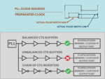
(2) MPW & Duty Cycle Degradation
Pic3 – Clock Duty Cycle Degradation
Clock waveform quality declines throughout the network due to “duty cycle degradation,” which lowers high or low pulse integrity. Major causes include:
.01 Low Pass Filter Effect – The clock or logic network functions as a series of RC filters, progressively reducing signal pulse width.
.02 Non-symmetrical Rise/Fall Delays – Real CMOS circuits often have uneven pull-up and pull-down strengths making rising edges propagate differently from falling edges and degrading the duty cycle over the network. This effect is modeled as process sigma variation in standard cell library. This cannot be credited as part of Common Path Pessimism Removal delay unlike nominal delays modeled by mean portion of standard cell delay.
.03 Loading Effect – Greater load in clock or logic stages slows edge transitions, increasing the time to cross the threshold and raising the minimum pulse width requirement.
.04 PVT Dependence – Low voltage (V) and high temperature (T) equates to weaker drive strength and smaller currents and makes the pulse width degradation worse.
.05 VT (channel length, threshold voltage) affects MPW requirements; shorter VT channel lengths need higher MPW requirement due to greater process variation, delay imbalance and short-channel effects.
.06 On Chip Variation Derates – Adjustments associated with process, voltage, temperature, distance based SOCV, wire, aging and radiation.
.07 Modeling Effects – Half Cycle Jitter narrows the effective clock pulse shape by altering its shape.
,08 Crosstalk – Any effective coupling on logical network will negatively impact each of rise/fall paths (both directions) and this incremental delay due to crosstalk does not cancel out as part of Common Path Pessimism Removal.
(3) MPW Slack Calculation
Pic4 – Clock Min Pulse Width High & LowPic5 – MPW Slack Calculation Details
Note: derates impact all delays compounded to cells/nets and not represented by a single value in equation and crosstalk delays not credited as part of CPPR credit for rise/fall and they impact slack negatively).
The first edge (rise for MPW high) is calculated as late as possible, and second edge (fall for MPW high) is calculated as early as possible. Since these semantics match setup style checks, MPW is normally reported in setup views. Doing these checks in hold views can produce optimistic results.
MPW is not reported on data and asynchronous pins. However dummy clock can be created on driver port to force tools to report MPW.
(4) MPW .lib (liberty format) syntax
A sincere attempt is made below to show the MPW spec as defined in library files (.lib liberty format) and brief explanation to interpret the same.
Pic6 – .liberty (.lib) syntax for MPW timing check
How MPW is characterized?
Minimum pulse width (MPW) characterization involves measuring the shortest pulse width for all clock and asynchronous set/reset pins. MPW is determined through a binary search, shrinking the pulse width until a failure criterion is met, i.e. either the output fails to switch, or the output peak voltage does not reach the required glitch-peak. This can be done by transistor level sub circuit extraction, applying input waveform of varying widths and sweeping across supply voltage, process corners and temperatures and measuring output.
During ETM generation, the MPW defined at the CK pin of the registers are transferred to the clock source port in ETM.
(5) How to Analyze & Fix MPW Violations
MPW timing should be verified thoroughly, regardless of whether the worst reported slack is positive. Additionally, MPW slack can be custom reported to a predefined list of endpoints (critical memories, output ports, custom IP pins etc.) to ensure comprehensive reporting without omissions.
Root Cause Analysis & Strategy To Avoid/Fix Violations
Accurate clock definition including waveform as it reaches MPW check endpoint.
Sometimes clocks are gated/regenerated and clock waveform modified before reaching destination pins. For slower L2/L3 memories where latency is less critical, the final clock may be set as Multicycle or Extended Pulse to relax MPW & Min Period constraint. Ensure generated clocks are accurately defined at right generated point without over-constraining MPW check. Hacking reports or waiving violations after being reported to compensate for inaccurate clock waveform definition is not efficient due to postprocessing effort and possibility of making errors.
Realistic MPW spec value as set by library or user definition
MPW high required value must be less than the clock pulse width high definition, besides accounting for half cycle jitter, duty cycle degradation, and derates. Otherwise, this might indicate improper memory configuration case analysis settings during memory compilation or linking of incorrect libraries. If so, review the conditional statements for the MPW spec in the .lib file and check proper library usage.
Also check to make sure right VT flavor of memory selected. Sometimes, lower VT memory must be selected at the expense of power to meet strict MPW spec.
Accurate half cycle jitter modeling, a function of pll jitter and clock network jitter components
During MPW signoff, select PLL jitter according to the appropriate PVT corner rather than using general approximations or a uniform specification for all timing corners. Next, ensure that the jitter resulting from clock propagation between the PLL source and its destination is thoroughly and accurately calculated (how CTS jitter is specified is beyond the scope of this article, but there is a structured way to generate this spec based on input slew, cell VT types, statistical foundry models and Monte-Carlo simulations). The final jitter should be determined either by conservatively summing the PLL jitter with the CTS network jitter or by employing RMS method (recommended) for greater accuracy. Additionally, it is important to confirm that the assumptions regarding top-level clock tree depth are correctly represented at the block level, thereby preventing any discrepancies at the top level.
Check accuracy of derates and margins applied
In MPW signoff mode, derates for aging, wire/RC, radiation, voltage, temperature and process (from library cell delay mean) are generally skipped, as source and destination clocks trace the exact path; only process derate sigma is excluded from CPPR credit if N and P device variation is modeled as process sigma component of cell delay. In this case, statistical variation is occurring at different edges and cannot assumed to be nullifying each other. Tools offer variables to control mean and sigma credit percentage, with some designers adding extra pessimism by not using CPPR credit. Not taking any CPPR credit is also very pessimistic. Always follow company guidelines based on thoroughly reviewed timing signoff spec. Usually this specification is defined by circuit and library teams based on earlier silicon feedback. Additional uncertainty may be used for min pulse width checks to safeguard against silicon failures. Setting proper derates is both an art and science balancing yield and time-to-market. Test chips can help refine derate specifications besides internal technical experiments and foundry suggestions. Note that CAD tools by default don’t consider clock uncertainty unless specific variables are set in timing analysis.
Clock Reconvergent Pessimism Removal – CRPR
When a clock reconverges to a clock pin via different launch and capture paths with clock distribution network, it may result in a pessimistic calculation of MPW slack. Timing tools provide variables to restrict MPW analysis to exact clock distribution pins on rise and fall timing paths thus eliminating any pessimism in MPW slack calculation
Assess the robustness of clock network, as it is the most significant factor influencing MPW
1 If clock paths do not use special CTS inverters that cancel out distortion or CTS-balanced buffers, distortion may occur; CTS should be repeated or ECOs applied.
2 Check for redundant DFT or power-saving clock gating and minimize gating in clock paths, as gating cells can disrupt duty cycle due to unequal rise and fall times.
These redundant gates cannot be detected by logic simulations. Special structural linting tools can identify these subtle issues.
3 Reducing insertion delay is important for achieving optimal MPW slacks. Ensure that the efficient routing layers are utilized besides best placement of cells in clock tree path.
5 Adhering to foundry and project specifications regarding cell use or recommended cell use is necessary to prevent the need for repeating Clock Tree Synthesis. Avoid high strength clock tree cells, which can cause Electromigration, and too weak clock tree cells, which are prone to crosstalk and noise
Crosstalk is also a major factor influencing MPW
Crosstalk, which is assessed under worst-case scenarios, can detrimentally affect both rise and fall transitions, CPPR credit is excluded for both rise and fall clock cells/nets that have crosstalk thus impacting maximum path width (MPW) slack. Leaf nets refer to the connections terminating at endpoint sequential device clock pins. Given their abundance, standard design practice typically refrains from shielding or double-spacing these nets, which results in unavoidable crosstalk. However, effective placement and routing utilization can help manage this limitation during the physical design closure phase. Nets not classified as “leaf nets” are considered clock trunk nets. These should remain entirely free from crosstalk by implementing measures such as double spacing, shielding, multi-layer routing, and avoiding the use of weak drive cells. Failure to do so has a direct effect on MPW slack. This aspect is frequently overlooked by Physical Design teams. Therefore, it is imperative to establish and enforce rigorous signoff criteria. Neglecting these standards may hinder the ability to meet MPW specifications.
PLL Placement – A key factor to reduce half cycle jitter
To minimize overall jitter, it is advisable to position the PLL at a location that is optimal for all modules traversed by the clock. This technique is essential; improper placement of the PLL may result in significant CTS delay, which can directly increase the jitter component, the non pll jitter component, within the CTS network.
In special cases, for example clocking high speed DRAMs, digital circuits to repair duty cycle are used. Another option is to use dual-phase clock distribution network. Rise/Fall edge are routed via identical clock trees and terminated by differential-single-ended signal. This is not very common in many SOCs.
MPW signoff checks during synthesis phase – a life saver
Design groups that do not perform MPW checks at the synthesis level may encounter significant issues and tapeout delays. Conducting MPW during the synthesis phase can help identify and address major architectural flaws early in the process. Providing feedback to architecture and library teams is a key aspect of this task at the synthesis stage. Also, adjusting MPW spec if needed. To support this, it is necessary to model CTS delays and derates with approximations.
Negotiate clock frequency as last resort
Reduce the clock frequency if conditions allow. Other methods may require significant resources and effort. In certain cases, internal clocks that interface with memory can be slowed by employing internally divided clocks, or by modifying the clock pulse shape before it reaches the relevant MPW assessed clock pins.
Conclusion
Failure to implement the MPW signoff methodology outlined above will lead to frequent bugs, negatively affect Time to Market, incur expensive design fix cycles, and diminish the credibility of the signoff process, which is the most critical factor.
Zameer Mohammed is a timing closure and signoff expert with over 25 years of experience, having held key technical lead roles at Cadence Design Systems, Apple Inc., Marvell Semiconductor, Intel, and Level One Communications. He specializes in STA signoff for complex ASICs, with deep expertise in constraints development and validation, synthesis, clock planning, and clock tree analysis. Zameer holds an M.S. in Electrical Engineering (VLSI Design) from Arizona State University and is a co-inventor on U.S. Patent No. 9,488,692 for his work at Apple. ( +1-512-200-5263 | linkedin.com/in/zameer-mohammed)
British-born, California-based entrepreneur, Gary Spittle, is the founder of Sonical – a disruptive, forward-thinking audio brand that is currently on the cusp of delivering something quite remarkable: think immersive, wireless, and completely lossless.
Gary holds a PhD. He investigated the use of binaural audio for improving conversations. He also holds numerous patents which help push forward innovations that make hearing technology more personal, flexible, and impactful.
What inspired you to launch Sonical, and what problem are you solving in the hearables space?
I founded Sonical in 2020 with the belief that our ears, and the devices we put in them, are the next frontier for personal computing. For decades, headphones and earbuds have been designed as simple sound making devices. Then Bluetooth and low power processing came along but the products remain closed systems, with fixed features defined by the product maker. This creates a barrier for innovation which prevents life-changing technology getting to the people that need it most. We saw an opportunity to create an entirely new product category, by building a platform that allows software developers to innovate directly for hearables, just as they do with smartphones.
Looking back since founding in 2020, what have been the most important milestones?
There have been several. Building our operating system, CosmOS, was a huge leap, it transforms hearables into open, upgradeable devices. Launching RemoraPro, our personal hearing computer with ultra-low-latency and lossless wireless audio streaming, demonstrated what’s possible when you reimagine the architecture of headphones. And now, with the support of Silicon Catalyst Venture, we’re moving from concept validation into scaling and commercialisation.
Technology & Differentiation
You’ve described Sonical’s vision as “Headphone 3.0.” Can you explain what that means for the industry?
Headphone 1.0 was wired and analogue, Headphone 2.0 was digital and wireless with Bluetooth. Headphone 3.0 is about hearing computers and putting the end user in control of what the product does – where hearables become intelligent, app-driven devices. Just like phones went from simple call-and-text machines to app ecosystems, headphones are on the same trajectory. CosmOS is the enabler – it allows multiple applications, from immersive audio to health monitoring, to run seamlessly on the same device.
How does your approach address issues like sustainability, longevity, and customisation in consumer devices?
Today’s headphones are often built to be low cost and have now reached a point where they are effectively disposable. They have the same limited features, short lifespans, and little scope for upgrades. With CosmOS, users can personalise their device through software, extending its value without replacing hardware. That means less waste, more choice, and new and better experiences over time. For manufacturers, it opens recurring revenue opportunities beyond hardware sales.
Market Opportunity & Partnerships
Hearables are forecast to become the next major personal computing platform. What evidence are you seeing to support that trend?
Already, wireless audio has become one of the most rapidly adopted consumer technologies. Market forecasts project the earbuds segment alone reaching over 1 billion units by 2030, and millions already use wireless headsets daily. Those numbers point to an opportunity: if hearables become more than just headphones – combining compute, context, sensing, and personalisation – they could emerge as a new personal platform. At the same time, advances in miniaturised sensors, AI, and low-power computing are turning the ear into a natural interface for health, productivity, and entertainment. We believe hearables will follow the same curve smartphones did, from a single-function product into a universal platform. The number of tech partners that want to work with us clearly supports this.
How do you envision app developers and partners contributing to this ecosystem?
Developers are the lifeblood of any platform. With CosmOS, they can create apps for everything from advanced audio experiences to wellness tools, without needing to redesign hardware. Our job is to give them the tools, APIs, and distribution channels to reach millions of users through a new type of product.
Can you share more about recent partnerships or pilots that highlight Sonical’s progress?
While some projects are still under NDA, I can say we’ve been working with world-leading audio brands, semiconductor companies, and health-tech innovators. Some of the software partners that we have announced publicly include Fraunhofer, Hear360, Oikla, Golden Hearing, Hear Angel and Idun Audio.
Technical Innovation
Your RemoraPro wireless technology enables ultra-low latency. What new applications does that unlock?
Latency is the lag between an audio event happening and the listener actually hearing it. This isn’t really a problem when you are just listening to music. But, for some applications such as gaming, watching movies or having conversations either in person or online, the delay can destroy the experience and in extreme cases make the product unusable. With RemoraPro, we’re achieving wireless latency so low it’s imperceptible. With CosmOS we also have the ability to process audio very fast which keeps the total system delay to a minimum. This unlocks new applications: musicians can perform wirelessly, gamers get instant feedback, and developers can deliver truly immersive sound environments.
Beyond audio quality, what advantages does RemoraPro bring to device makers and end users?
For product makers, RemoraPro is a complete solution that reduces integration time and complexity. For end users, it means access to new personalised experiences for the headphone products they already own. It also paves the way for new multi-channel and spatial audio use cases, which are game-changing for both creators and consumers.
Wellness & AI
You’ve talked about the ear as a gateway to wellness. What role can hearables play in areas like health and wellbeing?
The ear is an incredible point of access for biometric data. With the right sensors and algorithms, hearables can monitor heart rate, brain activity, stress levels, and even detect early signs of health conditions. Importantly, they can do this passively and discreetly, fitting seamlessly into daily life with a far greater accuracy than wrist worn devices.
At the same time, we see hearables playing a critical role in hearing protection. Millions of people, including children, already suffer from hearing damage, often leading to long-term challenges such as tinnitus. By enabling adaptive protection and personalised soundscapes, we can help reduce further damage while enhancing quality of life.
Another area we’re passionate about is specialised applications that are often overlooked. When product makers define the fixed features of a device, it’s difficult to justify niche use cases without making products prohibitively expensive. By opening up the platform through CosmOS, we allow developers to innovate directly for those needs, from professional audio tools to accessibility solutions, creating value where none existed before.
Sonical’s platform also uniquely brings together a wide spectrum of audio-related products, ranging from professional-grade devices to high-volume silicon and software systems. This breadth creates opportunities that few companies in the sector can match.
What types of AI-driven applications do you expect to see emerge first on CosmOS?
We are already seeing a blend of entertainment and wellbeing apps coming to the front. On one hand, personalised sound profiles, adaptive soundscapes, immersive audio, and AI-driven mixing tools. On the other, apps that help people manage stress, improve sleep, or support cognitive performance. The opportunity is vast, and embedded AI will be central to unlocking it.
Investment & Growth
Why was now the right time to partner with Silicon Catalyst ?
We’ve proven the hearing computer concept and secured strong technical and end user validation. Now it’s about scaling, building partnerships, and accelerating go-to-market. Silicon Catalyst and Silicon Catalyst Ventures not only provides capital, but also connects us to a network of executives, investors, and technologists who understand how to scale deep tech companies.
How will this investment accelerate your plans?
It allows us to expand developer engagement, strengthen pilot programs with hardware partners, and continue refining our technology stack. More importantly, it signals to the wider ecosystem that Sonical is a company to watch – we’re backed by investors and industry leaders who specialise in breakthrough technologies.
What does success look like for Sonical in the next 3 – 5 years?
Success is seeing CosmOS become the default platform for smart hearing products, just as Android and iOS became synonymous with smartphones. We want to enable a thriving developer community that unlocks completely new experiences for people that urgently need support, millions of users taking control of their hearing, and partnerships with the biggest names in audio, health, and computing.
Lessons from Bluetooth
You were part of the team that developed Bluetooth. What parallels do you see between that journey and Sonical’s vision today?
Bluetooth showed the power of an open standard to transform an industry. Back then, we had to convince the world that wireless connectivity could be reliable, affordable, and universal. With Sonical, the challenge is similar: we’re building the foundation for an entirely new ecosystem. The lesson is to think long-term, focus on putting the end user first, and create value for every stakeholder.
How are those experiences shaping the way you’re building the Headphone 3.0 ecosystem?
We know it takes more than great technology, you need the right partnerships, standards, and developer momentum. Bluetooth succeeded because we built a coalition. With Headphone 3.0, we’re applying the same approach: align the industry, unlock innovation with a large community of developers, and make it easy for consumers to adopt.
The History
Were there particular successes and failures from your past experiences that have shaped Sonical’s approach?
For sure. There is a common theme from the most successful projects I’ve worked on, that software is essential. More importantly, if you can enable others to develop on top of what you build it allows for differentiated products and new user experiences to be delivered. This drives higher customer satisfaction, expands the market and allows product makers to increase their pricing. I’ve seen the opposite happen too, where great products have failed due to lack of customisation or they were too complex which made them difficult to use.
Personal Motivation
On a personal note, what are you most proud of so far?
I’m proud that we’ve taken an ambitious vision and turned it into a platform that’s gaining real traction with global leaders. Building a team of brilliant engineers, securing top-tier partners, and earning investor confidence, that’s incredibly rewarding.
What keeps you motivated as you scale Sonical to the next stage?
The belief that we’re shaping the future of personal computing. If we succeed, headphones won’t just play music, they’ll become our most personal interface with technology. This elevates the device to a status where you won’t leave your home without it. That’s a once-in-a-generation opportunity, and seeing the impact we can have on individuals is what drives me every day.
Daniel is joined by Andrea Gallo, CEO of RISC-V International. Before joining RISC-V he worked in leadership roles at Linaro for over a decade and before Linaro he was a fellow at STMicroelectronics.
Dan explores the current state of the RISC-V movement with Andrea, who describes the focus and history of this evolving standard. Andrea describes the significant traction RISC-V is seeing across many markets, thanks to its ability to facilitate innovation. Andrea then describes the upcoming RISC-V Summit. He explains that the event will have many high-profile keynote speakers including Google and NASA, who will discuss RISC-V in space. Application of RISC-V to blockchain will also be discussed.
Andrea explains that there will be a new developers workshop on the first day of the summit which will include lectures and a hands-on lab with a real design. Exercises will include analyzing a SystemVerilog implementation to determine if a problem is in hardware or software. Other topics at the summit will include analyst presentations. Andrea also comments on the software enablement work underway as well as future expansion of RISC-V.
The RISC-V Summit will be held at the Santa Clara Convention Center on October 21-23. (October 21 is Member Day.) You can get more information and register for the event here.
The views, thoughts, and opinions expressed in these podcasts belong solely to the speaker, and not to the speaker’s employer, organization, committee or any other group or individual.
In a move that underscores the semiconductor industry’s push toward resilient supply chains and agile innovation, Thalia Design Automation and X-FAB Silicon Foundries have announced a strategic partnership aimed at safeguarding supply continuity and accelerating intellectual property (IP) migration. This collaboration, revealed on September 23, 2025, comes at a pivotal moment when end-of-life (EOL) process technologies and geopolitical tensions are disrupting global chip production, forcing companies to rethink their design lifecycles. By integrating Thalia’s AI-driven migration tools with X-FAB’s specialty manufacturing expertise, the alliance promises to empower customers—particularly in automotive, industrial, and medical sectors—to transition designs swiftly without compromising performance or incurring prohibitive costs.
Thalia Design Automation, a UK-based venture-funded EDA (electronic design automation) specialist, has emerged as a key player in analog, mixed-signal, and RF IP solutions since its founding in 2012. Headquartered in Cwmbran, Wales, with additional facilities in Hyderabad, India, and Cologne, Germany, Thalia focuses on automating the complex task of porting legacy designs to newer processes. Its flagship AMALIA Platform leverages artificial intelligence to handle layout optimization, parameter extraction, and validation, slashing migration times from months to weeks. Backed by $2.7 million in funding in 2023, Thalia has positioned itself as a bridge between outdated silicon nodes and future-proof technologies, addressing a market gap where manual redesigns often lead to errors and delays. CEO Sowmyan Rajagopalan has emphasized the company’s mission: “In an era of supply volatility, our tools aren’t just about migration—they’re about survival and scalability.”
Complementing Thalia’s software prowess is X-FAB, a global leader in analog/mixed-signal semiconductor foundries. Established in 1992 as a spin-off from Siemens, the Erfurt, Germany-based group operates as a pure-play foundry, fabricating custom chips without competing in end markets. With fabrication sites in Germany, Malaysia, the US, and Canada, X-FAB specializes in mature process nodes (0.35µm to 1µm) tailored for harsh-environment applications like power management, sensors, and MEMS devices. Serving over 200 customers worldwide, the company reported steady growth in its 2024 Investor Day, highlighting a focused strategy on three technology pillars: high-voltage, RF, and silicon carbide. X-FAB’s emphasis on long-term support for legacy processes makes it an ideal partner for migration efforts, as it helps clients avoid the pitfalls of abrupt supplier shifts.
At the heart of this partnership is a symbiotic integration: Thalia will access X-FAB’s comprehensive Process Design Kits (PDKs), enabling the AMALIA Platform to be fine-tuned for X-FAB’s diverse portfolio of specialty technologies. This allows for automated, silicon-proven porting of analog and mixed-signal IPs, ensuring designs retain critical metrics like noise margins, power efficiency, and thermal stability during transitions. Customers benefit from reduced engineering overhead—traditional migrations can cost millions and take up to a year—while gaining qualification-ready outputs that accelerate time-to-market by 50-70%, according to Thalia’s internal benchmarks.
The strategic value extends beyond technical efficiencies. In an industry reeling from the 2021-2023 chip shortage and ongoing US-China trade frictions, this alliance fortifies supply chain resilience. By offering a “second-source” migration pathway, it mitigates risks from EOL announcements, which affect up to 30% of legacy designs annually. For X-FAB, it bolsters customer retention; as COO Damien Macq noted, “This partnership enhances customer confidence, securing long-term supply and supporting the full lifecycle of our specialty technologies.” Rajagopalan echoed this sentiment: “Combining our AI automation with X-FAB’s manufacturing excellence lets customers adapt to market shifts while unlocking advanced process benefits.”
Broader implications ripple across the semiconductor ecosystem. As electric vehicles, 5G infrastructure, and IoT devices demand ever-reliable analog components, partnerships like this could standardize migration practices, potentially inspiring similar tie-ups with other foundries like GlobalFoundries or TSMC. Analysts predict the IP migration market will grow to $5 billion by 2030, driven by AI tools that democratize access to advanced nodes. For smaller fabless firms, often squeezed by big-tech dominance, Thalia-X-FAB provides a lifeline to innovate without starting from scratch.
Ultimately, this collaboration exemplifies proactive adaptation in a volatile sector. By prioritizing supply security and migration speed, Thalia and X-FAB not only protect their partners’ bottom lines but also pave the way for sustainable growth. As supply chains evolve, expect more such alliances to emerge, ensuring the analog world remains robust amid digital disruption.
In the business press today I still find a preference for reporting proof-of-concept accomplishments for AI applications: passing a bar exam with a top grade, finding cancerous tissue in X-rays more accurately than junior radiologists, and so on. Back in the day we knew that a proof-of-concept, however appealing, had to be followed by the hard work required to transition that technology to a scalable solution, robust in everyday use across a wide range of realistic use cases. A less glamorous assignment than the initial demo, but ultimately the only path to a truly successful product. The challenge in productization for AI-based systems is that the front-end of such products intrinsically depends on a weak component: our imperfect directions to AI. I recently talked to David Zhi LuoZhang, CEO of Bronco AI, on their agentic solution for verification debug. I came away with a new appreciation for how scaling our learned debug wisdom might work.
The challenge in everyday debug
When we verification types think of debug challenges we naturally gravitate towards corner case problems, exemplified by a strange misbehavior that takes weeks to isolate to a root cause before a designer can even start to think about a fix.
But those cases are not what consume the bulk of DV time in debug. Much more time-consuming is triage for the hundred failures you face after an overnight regression, getting to first pass judgment for root causes and assigning to the right teams for more detailed diagnosis. Here some of the biggest time sinks more likely come from mis-assignments rather than from difficult bugs. You thought the bug was in X but really it was in Y or in an unexpected interaction between Y and Z.
How do DV teams handle this analysis today? It’s tempting to imagine arcane arts practiced by seasoned veterans who alone can intuit their way from effects to causes. Tempting, but that’s not how engineering works and it would be difficult to scale to new DV intakes if they could only become effective after years of apprenticeship. Instead DV teams have developed disciplined and shared habits, in part documented, in part ingrained in the work culture. Consider this a playbook, or more probably multiple playbooks. Given a block or design context and a failure, a playbook defines where to start looking first, what else to look at (specs, RTL, recent checkins, testbench changes, …), what additional tests might need to be run, drilling down through a sequence of steps, ultimately narrowing down enough to likely handoff targets.
Tough stuff to automate before LLMs and agentic methods. Now automating a significant chunk of this process seems more within reach.
The Bronco.ai solution
The Bronco solution is agentic, designed to consume overnight regression results, to triage those result down to decently confident localizations, and to hand off tickets to the appropriate teams.
Playbooks are learned through interaction with experienced DV engineers. An engineer starts with a conversational request to Bronco AI, say
“I want to check that my AES FSMs are behaving properly. Check for alerts, interrupts, stalls, and that the AES CTR counter FSM is incrementing for the right number of cycles”
The engineer also provides references to RTL, testbench, specs, run log files, waveforms and so on. The tool then suggests a playbook to address this request as a refined description of the requirement. The engineer can modify that refined version if they choose, then the tool will execute the playbook, on just that block if they want, or more comprehensively across a subsystem or the full design and then will report back as required by the playbook. During this analysis, Bronco AI will take advantage of proprietary AI-native interfaces to tap into tool, design, spec and other data.
Playbooks evolve as DV experts interact with the Bronco tools. David was careful to stress while the tool continuously learns and self-improves through this process, it does not build models around customer design or test data but rather around the established yet intuitive debug process (what David calls the “Thinking Layer”), which becomes easier to interpret and compartmentalize (and if needed can be forgotten).
He also clarified an important point for me in connecting specs to RTL design behavior. There is an inevitable abstraction gap between specs and implementation with consequent ambiguity in how you bridge that gap. That ambiguity is one place where hallucinations and other bad behaviors can breed. David said that they have put a lot of work into “grounding” their system’s behavior to minimize such cases. Of course this is all company special sauce, but he did hint at a couple of examples, one being understanding the concept of backtracking through logic cones. Another is understanding application of tests to different instantiations of a target in the design hierarchy, obvious to us, not necessarily to an AI.
The Bronco.ai philosophy
David emphasized that the company’s current focus is on debug, which they view as a good motivating example to later address other opportunities for automation in verification and elsewhere in the design flow He added that they emphasize working side by side with customers in production, rather than in experimental discovery in pre-sales trials. Not as a service provider, but to experience and resolve real problems DV teams face in production, to refine their technology to scale.
I see this as good progress along a path to scaling debug wisdom. You can connect with Bronco.ai starting HERE.
David Zhi LuoZhang is Co-Founder and CEO of Bronco AI with extensive experience in building AI systems for mission-critical high-stakes applications. Previously while at Shield AI, he helped train AI pilots that could beat top human F-15 and F-16 fighter pilots in aerial combat. There, he created techniques to improve ML interpretability and reliability, so the system could explain why it flew the way it did. He gave up a role at SpaceX working on the algorithms to coordinate constellations of Starlink satellites in space, and instead founded Bronco to bring AI to semiconductors and other key industries.
Tell us about your company.
We do AI for design verification. Specifically, we’re building AI agents that can do DV debugging.
What that means is the moment a DV simulation fails, our agent is already there investigating. It looks at things like the waveform, the run log, the RTL and UVM, and the spec to understand what happened. From there, it works until it finds the bug or hands off a ticket to a human.
We’re live-deployed with fast-moving chip startups and are working with large public companies to help their engineers get a jump on debugging. And we’re backed by tier-1 Silicon Valley investors and advised by leading academics and semiconductor executives.
What problems are you solving?
If you look at chip projects, verification is the largest, most time-consuming, and most expensive part. And if you look at the time-spent of each DV engineer, most of their time is spent on debug. They are watching over these regressions and stomping out issues as they show up over the course of the project.
Every single day, the DV engineer gets to work and they have this stack of failures from the night’s regression to go through. They have to manually figure out if it’s a design bug or a test bug, if they’ve seen the bug before, what the root cause might be, and who to give it to. And this is quite a time-consuming and mundane debugging process.
This creates a very large backlog in most companies, because typically this task of understanding what’s happening in each failure falls onto a select few key people on the project that are already stretched thin. Bronco is helping clear this bottleneck and take the pressure off those key folks and in-so-doing unblock the rest of the team.
What application areas are your strongest?
We focus on DV debug. We chose DV debug because it is the largest pain point in chip development, and because from a technical standpoint it is a very strong motivating problem.
To do well at DV debug, we need to be able to cover all the bases of what a human DV is currently looking at and currently using to solve their problems. For example, we’re not just assisting users in navigating atop large codebases or in reading big PDF documents. We’re also talking about making sense of massive log files and huge waveforms and sprawling design hierarchies. Our agent has to understand these things.
This applies at all levels of the chip. With customers, we’ve deployed Bronco everywhere from individual math blocks up to full chip tests with heavy NoC and numerics features. One beautiful thing about the new generation of Generative AI tools is that it can operate at different levels of abstraction the same way humans can, which greatly improves its scalability compared to more traditional methods that would choke on higher gate counts.
What keeps your customers up at night?
It’s a well-known set of big-picture problems that trickle into day-to-day pains.
Chip projects need to get to market faster than ever, and the chips need to be A0 ready-to-ship, but there just aren’t enough DV engineers to get the job done.
That manifests in there not being enough engineers to handle the massive amount debugging that needs to go into getting any chip closed out. So the engineers are in firefighting mode, attacking bugs as they come up, and being pulled away from other important work – work that could actually make them more productive in the long-run or could surface bigger issues with uncovered corner cases.
And moreover, this burden falls most heavily on the experts on the project. During crunch time, it’s these more experienced engineers that get inundated with review requests, and because of institutional knowledge gaps, the rest of the team is blocked by them.
What does the competitive landscape look like and how do you differentiate?
There are the large EDA giants, and there are a few other startups using AI for design and verification. Most of their work focuses on common DV tasks like document understanding and code help. These are general, high surface area problems that aren’t too far from the native capabilities of general AI systems like GPT.
No other company is taking the focused approach we are to AI for DV. We are focused on getting agents that can debug very complex failures in large chip simulations. We use that actually as a way to define what it means to be good at those more general tasks in the DV context like understanding spec docs or helping with hardware codebases.
For example, it’s one thing to answer basic questions from a PDF or write small pieces of code. It’s another thing to use all that information while tracing through a complex piece of logic. By taking this focused approach, we’re seeing huge spillover benefits. We almost naturally have a great coding assistant and a great PDF assistant because they’ve been battle-tested in debug.
What new features or technology are you working on?
All of our tech is meant to give your average DV engineer superpowers.
On the human-in-the-loop side, we are making a lot of AI tools that automate the high-friction parts of manual debug. For example, our tool will go ahead and set up the waveform environment to focus on the right signals and windows, so engineers don’t have to spend ridiculous amounts of time clicking through menus.
On the agent side, we want to allow each DV engineer to spin up a bunch of AI DVs to start debugging for them. That requires a really smart AI agent with the right tools and memory, but also really good ways for users to transfer their knowledge to the AI. And of course, we are doing all this in a safe way that stays on-premise at the customer’s site to put their data security first.
And we’re doing all these things on ever-larger and more sophisticated industry-scale chip designs. In the long term, we see a large part of the Bronco Agent being like a scientist or architect, able to do very large system-level reasoning about things like performance bottlenecks, where the Agent has to connect some super high-level observation to some super low-level root cause.
How do customers normally engage with your company?
Customers have a very easy time trying our product, since we can deploy on-prem and can leverage existing their AI resources (eg. Enterprise ChatGPT). First, the customer chooses a smaller, lower-risk block to deploy Bronco on. Bronco deploys on-premise with the customer, typically via a safe, sandboxed system to run our app. Then, Bronco works with the block owner to onboard our AI to their chip and to onboard their DVs to our AI.
From there, it’s a matter of gauging how much time our AI is saving the DV team on tasks they were already doing, and seeing what new capabilities our tool unlocked for their team.