Shooting beyond the hill…
In former times (think WW1 before GPS and satellites), an artillery battery trying to shell targets out of sight behind a hill would have to rely on an approximate grid reference and a couple of soldiers on top of the hill (who could see the target) to tell them where the shots were landing. These range finders would semaphore back to the battery telling them to adjust range and direction until they were on target. A process of successive refinement, which shares much in common with the search for Power Bugs!
Trying to identify where to find power bugs suffers from similar limitations; very often the target area may not be known at all, or least only be approximated. Surveys show that over 80% of designs are now actively managing power in some way. Missing your power targets can be catastrophic, especially if this is only realized when you get silicon back. Power has never been more important.
Power Matters! Applications drive real power needs…
A product-level power requirement example might be that the user should be able to watch Netflix for 15 hours on a full charge. This determines the chip-level power targets, which in turn determines the sub-system and block-level power targets. To meet this “15 hours of Netflix” requirement, you will need to be able to perform power analysis from the chip-level downwards and validate that power targets are being met under the conditions of this real workload. For complex ASIC devices, you really need to run the full system software in order to see what is going on power-wise under the target operating conditions.
Short, directed test sequences cannot predict accurately how the device will behave under more complex conditions.
Hit the target – Why use emulation for power analysis?
When it comes to finding power bugs, the first step is to find the right platform. All SOC/ASIC product developments are a combination of software development and hardware development. Power management capabilities are provided by the hardware and controlled by the software, so both must be validated, and the power bugs can be on both sides.
Hardware Emulation systems are effective and performant platforms for software development in advance of available hardware reference boards, system-level validation demonstrating that the hardware with the target firmware/software delivers the required capabilities, system-level verification bug searching/hunting from a system context, and also system-level power verification (achieved through power analysis capabilities). We will talk about the role of emulation not only for the well-known generation of design activity but also from the perspective of an integrated power analysis flow.
Power analysis using emulators with multi-MHz performance, support for checkpoint-restore, system-level debug, and fast power analysis turnaround times, is the only way to achieve this by running the full system or substantial sub-system software enabling designers to perform:
fast “silicon-approximate” power consumption analysis tested on a real-world system workloads
So, what are Power Bugs?
We consider power bugs in the context of any error (hardware or software) in the product, no matter if it results in an observable functional error (a more traditional bug perhaps), or a failure to meet power consumption (or power drain) objectives and targets. Either way, the result is the same; an error or omission in either the hardware (as RTL, power intent (UPF) or implementation), or the power management software (firmware/device drivers), which must be fixed. The fix must then be re-validated.
We are treating both functional power bugs and power consumption problems as “Power Bugs”. Power Bugs really fall into 2 categories…
Power Management causes a functional failure
This category of power bugs is related to function, but that functionality is associated with power management and is described by both RTL and power intent code. Examples could be, an incorrect behavior in power controller logic (which may contain complex Finite-State-Machines and control logic), or a functional error in clock-gating logic, an error in power domain logic (or associated isolation or retention logic), or Dynamic Voltage and Frequency Scaling (DVFS) control logic.
A missed critical low-power bug could result in functional failure of your first silicon the worst scenario.
That’s a very expensive mistake, but it has happened!
Too much power is consumed
For those Power Bugs that do not present as an observable functional error, you really have to adopt a power analysis approach to Power Bug hunting. We refer to these bugs as “power consumption bugs”. They are errors in the measured power drain in relation to the expected or estimated power, possibly arising from errors, omissions or missed opportunities in either the RTL, or power intent (UPF).
Serious power consumption bugs can render the final product less-competitive, or non-viable in the worst case.
Imagine that you have implemented a range of low-power capabilities and tested them all thoroughly, all the software is working, but the first silicon is measured to be consuming 30% more power than expected. That has also happened!
Classes of Power Bugs
Given the two categories described above, we can further enumerate Power Bugs into the following bug classes:
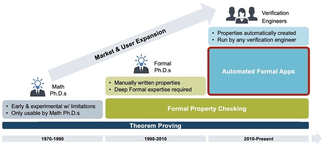
Modern ASIC power verification is many-layered. Low-power architectures must be considered and evaluated right at the start of the specification and the high-level design processes. It cannot be left as an implementation process as that will be far too late! Many traditional verification workflows have been enhanced to be “power-aware”, and some new ones that have been created to statically analyze power-intent. It can start long before RTL is written, using power-aware virtual prototyping. With a VP, you have a capability to dynamically explore different low-power architectures at the system level whilst running development power management software. While accurate power analysis is not possible, relative estimates of power consumption are. It enables designers to explore the hardware/software split, develop and debug early power management software, and use high-level power intent to model power architectures.
Power aware verification…virtually
Early power estimates can feed-forward to the RTL development workflows.
As early RTL is developed and the power intent is refined, you need workflows that will enable early RTL power estimation so that you can keep track of power consumption throughout development and use power analysis to refine microarchitecture design choices. There are power-aware static analysis workflows and power-aware simulation workflows that support this phase of development. As we know, simulation testbench environments are well suited to short directed and constrained-random test vectors, with the benefit of coverage and assertions, and with a gold-standard debug environment; running the real software is not generally feasible. However, there will be a class of Power Bug that can only be found when you are running the real software in a system environment,
that emulates realistic I/O traffic, and with realistic power transition sequences under the control of the actual (or close to actual) system power management software. We will refer to this as “software-driven power verification”.
Why Software-Driven Power Verification?
ASIC pre-silicon validation demands that at some point you need to validate the full system hardware model with the target firmware and software. Emulation offers fast initial compile and bring-up, fast turnaround time as the RTL changes, advanced RTL debug capabilities and delivers up to a few MHz levels of runtime performance. This is enough to be able to compile your RTL, boot your OS, run applications and perform RTL debug well within the working day, opening up the ability to find power bugs that are only observed when running system software testing workloads.
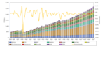
Source – Acuerdo and Valytic Consulting
Software test workload #4 above clearly shows some unexpected power consumption that might arise from 2 different power bugs. The root causes could be hardware or power management software. Debug will determine.
Scale-up and Speed-up
Emulators can model large design sizes which enables you to,
“scale-up” verification to the full system.
In addition, modern emulators provide power analysis workflows that allow you to extend your power analysis from the constraints of short simulation sequences, to the billions of cycles consumed when running the actual software enabling the user to,
“speed-up” detailed power analysis over large samples of system software.
Users generally need the following capabilities and outputs that emulation power analysis offers.
- Visualization of power activity across billions of cycles. Accuracy is less critical but relative activity should accurately guide the user to identify power-critical time-windows of interest.
Source – Acuerdo and Valytic Consulting
- Ability to measure the average power for power-critical time-windows. Emulator power analysis workflows do this by generating standard Switching Activity Interchange Format (SAIF) data which can be processed by power sign-off tools to compute average power data.
- Calculation of cycle-by-cycle power waveforms for power-critical time-windows, in order to debug Power Bugs and identify shorter power sign-off windows.
- Calculation of peak power. Emulator power analysis workflows do this by generating waveform files (e.g., VCD, FSDB) that can be processed by power sign-off tools to compute peak-power.
Source – Acuerdo and Valytic Consulting
- Ability to increase the fidelity of the analysis by performing the power analysis using RTL, post-synthesis netlists and post place-and-route netlists. Post place-and-route analysis should be able to consume real timing data (SDF), real network capacities data (SPEF) and technology library data (.lib)) and achieve full accuracy power sign-off.
Turnaround time is critical
What matters here is the end-to-end turnaround time from RTL compile to running the payload, and then extracting, processing and analyzing the power data. Fast turnaround times make many iterative power analyses feasible. Emulation power analysis can generate terabyte volumes of data per run. This data has to be processed using scalable compute grids to slice and process the data in order to generate the average power and the cycle power curves.
This data-processing part of the workflow is time-critical and requires scalable compute.
Booting the operating system could account for the first 30 billion cycles, and that might not be the region of most interest system activity-wise. You might then be looking at billions of further cycles to analyze interesting power-critical windows where more functionality is active.
Emulation checkpoint and restore capability allow you to jump to a power-critical timepoint of interest for targeted power analysis.
Developers need to be able to cycle through multiple turns of the power verification workflow per day. The hardware developers may need to re-verify a change to the RTL or the power intent. The software team may need to re-verify a patch to the power management code and get the result back within the same day. Additionally, it is highly likely that there are multiple power-critical windows that need to be analysed when performing power analysis over multi-billion cycle windows.
Software-driven power verification using emulation is the only way to achieve this pre-silicon, by running the full system (or substantial sub-system) software.
Beyond using emulation, the only way to get closer to real systems is with actual silicon, by which time it is too late to make power design choices and to find power related bugs in the hardware.
Finally, some things to remember…
Plan to Succeed
As with any other verification challenge, you need to start with a test plan. What strategies are you going to apply to power validation and hunting for Power Bugs?
Don’t leave power verification to chance; brainstorm, review and refine your test plan just as you would for any other class of verification
Power verification should be a chapter in an overall verification test plan and together with a decision on the tools and methodologies you are going to apply to the problem. There should be power targets or objectives that will need to be validated, and scenario planning of the set of sequences and power modes that need to be exercised.
Power regressions
Performance and power are in a constant trade-off. Increasing performance often implies adding more logic, replicating structures, and controlling fan-out with additional buffers to reduce logic depth between flops. Hence there is a need to perform power analysis regressions to keep checking that iterative refinements of the design, do not cause power bugs to be introduced as power is unintentionally negatively impacted.
Power data analytics
As with all other aspects of verification, power analysis regressions will generate power datasets that need to be stored, maintained, visualized and explored. Look at the trends for max power and average power results, both at the top-level and hierarchically, to track progress over time as the RTL code is developed and refined.
In order to improve, you have to measure.
The power metrics are just another dataset that you will need to track alongside all other design and verification metrics. Ideally, your data analytics platform will support the cross correlation of power metrics with other key metrics such as performance and area, bug rates, and code churn rates. When you look at all of these measurements in the round, great insights are possible.
Read the full whitepaper “Power Bug Quest” for a more detailed analysis of finding Power Bugs using software-driven power analysis.


