This is not about architecting a full SoC from scratch. You already have a competitive platform, now you want to add some kind of accelerator, maybe video, audio, ML, and need to explore architectural options for how accelerator and software should be partitioned, and to optimize PPA. Now we have AI to help us optimize you’d like to run multiple experiments to drive training, from which you can find an optimum to meet your needs.
Challenges for AI-based automation
Reinforcement learning methods are already popular at the back end of design, for optimization against multi-physics analytics as one example. There analysis is very time consuming, so learning leverages a sparse set of sample states, yet the method still delivers meaningful optimization, for thermal among other parameters.
However, optimization for architectural design must explore a much more diverse and rich design space. How many ways can you build an AI accelerator or an MPEG codec? Reinforcement learning here must run over a denser sampling of the design space. Parameter sweeps are too expensive; reinforcement learning instead starts with initial sample states and follows paths towards maximizing a reward function, perhaps over hundreds or even thousands of samples.
This level of sample counts requires that the method to compute a cost function (to first order based on area and timing) must be fast. But equally it must be reasonably accurate, correlating decently well with costs you would get from a production analysis, otherwise fast optimization is meaningless.
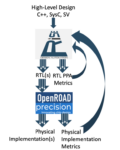
The class of architectures we’re considering is most likely to start in software, MATLAB or similar models, to support fast prototyping against realistic application loads. Mapping to hardware for exploration trials will go through C++, System C, or perhaps behavioral SystemVerilog depending on architect/designer preference. Then through high-level synthesis (HLS) to implementable RTL. From there on to implementation: physical synthesis and further if needed to provide cost feedback to reinforcement learning. Cost functions are computed after HLS, also after physical implementation, feeding back to the next round of learning.
Rise DA in partnership with Precision Innovations
This HLS step is an obvious area of strength for Rise DA, who cite they are 10x faster than other HLS tools. They also cite correlation with customer post-synthesis results to within 10% in most cases, thanks to built-in critical path RTL synthesis insight.
While Rise can and does support any RTL synthesis and implementation tool in their flow, the Precision Innovation partnership adds fast implementation estimation data, leveraging the open-source OpenROAD platform (developed in UCSD). Precision position themselves as the Redhat/SUSE parallel to OpenROAD, as OpenROAD is parallel to Linux. Precision cites within 5% accuracy on area and 20% accuracy on timing, with results verified down to 12nm for tapeouts and down to 2nm for estimation. Precision cites 4-20x faster throughput than proprietary tools.
On correlation, Allan Klinck (co-founder at Rise DA) supported by Tom Spyrou (CEO at Precision), add that in many cases Rise see performance correlation within a few percent because they are micromanaging the architecture mapping without needing to add cheat cells. Not surprising to me since these days performance is heavily influenced by architecture. Equally, Tom says that they do not see significant variance by PDKs, even down to 2-3nm. (For Rise, area correlation can show more variance thanks to factors outside their control, like memory sizes.)
In this partnership both ventures also offer a creative licensing model. Licensing is based on number of users and blocks, not number of parallel runs. You can run as many jobs in parallel as you want, especially important in view of learning applications.
Agentic support
Allan added that reinforcement learning is accomplished through an agent, also they offer a design agent. Starting from requirements prompts, it calls the RISE tools to synthesize an untimed design, which can then be refined interactively. That design can be fed into the design-space exploration agent to optimize PPA or used as-is.
I like it. A creative combination of high-level synthesis coupling to a proven open-source RTL2GDS supported by Precision Innovations, together supporting an AI learning-friendly license model. You can learn more about Rise DA HERE, Precision Innovations HERE, and the OpenROAD project HERE.
Also note that Rise and Precision plan a webinar in February 2026.
(OpenROAD was developed by the team now at Precision Innovations while they were funded by DARPA/UCSD, and they continue to contribute to its evolution.)
Also Read:
Rise Design Automation Webinar: SystemVerilog at the Core: Scalable Verification and Debug in HLS