By Vikash Kumar, Senior Verification Architect | Arm | IEEE Senior Member.
The Problem Every Verification Engineer Recognizes
You ask an LLM to generate a UVM testbench. It produces 25 files. Everything compiles. You run the simulation — and nothing happens. The scoreboard reports zero checks. The slave driver stops after 10 transactions. The simulation hangs.
This is not a hypothetical. In a controlled experiment generating a UVM testbench for an AHB2APB bridge using a state-of-the-art commercial LLM, this is exactly what happened — after an automated agentic repair loop had already resolved 37 compile errors across 4 iterations.
The core problem: compile success is nearly uncorrelated with functional correctness at the protocol level. Yet compile success is the dominant evaluation metric in LLM-for-hardware research. This article explains why that is the wrong metric, what the right metrics are, and what it means for verification teams trying to use LLMs in production.
What Compile Success Actually Tells You
A compiler verifies type consistency, scope resolution, and syntactic validity. It does not verify protocol timing, handshake sequencing, interface role semantics, or transaction counting.
Here are three failures from the AHB2APB case study — each catastrophic to verification, none producing a compiler error:
Role confusion: The LLM generated an APB slave driver that drives PADDR, PSEL, and PENABLE — the master’s outputs. An APB slave only drives PRDATA, PREADY, and PSLVERR. The simulation ran without complaint. The slave simply never responded.
Timing phase error: The AHB driver presented HWDATA in the same clock cycle as HADDR. AHB requires a one-cycle offset — HWDATA is valid in the cycle after HADDR. The testbench drove the wrong data on every single transaction.
Response deadlock: The master sequence called get_response() waiting for the driver to call put_response(). The driver never called it. The simulation hung silently at transaction 1.
A controlled taxonomy of eight failure modes from the case study breaks down as follows: one was detectable at compile time (L2: hallucinated sequence item field names), one surfaced at elaboration during VIF port resolution (L1), and six required simulation or waveform analysis to diagnose (L3–L8). The compiler caught one of eight.
Three Metrics That Actually Measure the Gap
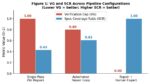
Repair Efficiency Score (RES)
RES = total compile errors / total repair calls. In the case study, 37 errors resolved in 15 calls gives RES = 2.47. A single repair call that fixed hallucinated sequence item field names collapsed 18 downstream errors simultaneously — demonstrating that errors cluster around shared root causes when an LLM misunderstands a core abstraction.
Verification Gap (VG)
VG is the fraction of functional failures that survive a compile-clean testbench. VG = 0.00 means the testbench is both compile-clean and functionally complete. VG = 0.80 after the automated repair loop means 80% of functional failures remained after full automation — invisible to the compiler throughout. This is the metric the field is not computing.
Specification Coverage Ratio (SCR)
SCR measures what fraction of the protocol specification the testbench actually exercises. A testbench covering only happy-path transactions — missing burst-interrupt termination, error-retry, and maximum-wait-state scenarios — can have SCR well below 1.0 while passing all simulation checks on normal traffic.
The Fix Is a Better Specification, Not a Bigger Model
The most counterintuitive finding from this study: the highest-leverage investment to improve LLM-based verification automation is not a more capable model. It is a more formal specification schema.
Timing phase failures exist because specifications encode timing in natural language: ‘HWDATA is valid one cycle after HADDR.’ No amount of model scale resolves the ambiguity between that prose and the precise simulator semantics of @(posedge HCLK) sequencing.
A manifest field encoding HWDATA_phase_offset: 1 gives the generation agent an unambiguous directive — the failure becomes preventable rather than debuggable. Role confusion failures become preventable if the manifest classifies interface roles explicitly: apb_slave: {role: reactor, perpetual: true}. In both cases, the fix is upstream specification formalization, not downstream repair.
Eight of approximately 25 generated files required complete expert rewrites to achieve functional correctness. Every one of those rewrites addressed a failure the compiler never flagged.
The Real Bug the Testbench Found
After achieving functional correctness through expert collaboration, 30 randomized AHB transactions detected a previously unknown RTL race condition in the bridge’s xfer_pending clearing logic.
The bridge uses a registered clear that activates one clock cycle too late. The FSM reads stale xfer_pending = 1 and re-enters APB_SETUP, generating a phantom APB transfer with the previous transaction’s latched address. The scoreboard detected 6 PSEL assertions for 5 AHB transfers — a 1:1 AHB-to-APB ratio violation invisible to IP-level simulation.
This is precisely the class of integration bug that protocol-level testbench modeling exists to find — and it is why getting the testbench right matters. A compile-clean testbench with VG = 0.80 would never have run the checks that found it.
What This Means for Your Verification Flow
If you are evaluating LLM-based testbench generation tools, ask the vendor: what is your Verification Gap on a real protocol design? Compile success is not evidence of a working testbench. RES, VG, and SCR are.
If you are integrating LLMs into your verification flow, the eight-failure taxonomy gives you a concrete checklist. Check for role confusion in every driver. Check for timing phase errors at every AHB and APB interface. Check for liveness failures in every sequence that is supposed to run indefinitely. Check the elaboration log — not just the compile log.
If you are writing the specification that feeds the LLM, encode timing constraints, interface roles, and behavioral contracts as structured fields — not prose. The gap between compiles and verifies is the gap that matters. Start measuring it.
About the Author
The author is a Senior Verification Architect at Arm and an IEEE Senior Member, with 15+ years of experience in hardware verification including prior work at Intel. Specializes in subsystem-level verification for chiplet-based designs and protocol verification (AHB, AXI, CHI, PCIe, UCIe). Active in IEEE standards and peer review activities.
Also Read:
Building the Interconnect Foundation: Bump and TSV Planning for Multi-Die Systems
Designing the Future: AI-Driven Multi-Die Innovation in the Era of Agentic Engineering
Accelerating Static ESD Simulation for Full-Chip and Multi-Die Designs with Synopsys PathFinder-SC