The semiconductor industry is in the midst of a structural supply challenge that’s tightly coupled to exploding demand for advanced chips, especially those used in AI, HPC, and next-generation mobile and consumer devices. At the center of this vortex is the 2nm class of manufacturing technology, representing one of the most complex and expensive transitions in semiconductor history due to its reliance on nanosheet or GAA transistor architectures and extremely precise lithography tools.
TSMC and the 2 nm Capacity Crunch
TSMC’s N2 process node officially entered volume production in late 2025, and early estimates of yield and ramp have been strong enough that the company is aggressively increasing capacity. N2 promises up to 15 % performance gains or substantial power reductions versus previous nodes, making it extremely attractive for next-generation AI accelerators and flagship mobile chips.
The demand has been remarkable! Reports from the trenches indicate that much of TSMC’s N2 capacity is effectively sold out through 2026, with major customers like Apple, Nvidia, Qualcomm, and AMD reportedly locking in large shares of the initial output. This is partly because modern AI accelerators require much more wafer real estate per chip than traditional mobile processors, which exacerbates capacity constraints.
To meet this demand, TSMC has outlined plans to expand production aggressively across multiple fabs, including Hsinchu Baoshan and Kaohsiung in Taiwan and other international sites, with targets that could see monthly wafer starts reach well into six figures by 2026–2028. TSMC’s CAPEX is also a tell for things to come. In 2024 it was $29.8 billion, 2025 a 37% increase to $40.9 billion and a record $52-56 billion in 2026. What this tells me is that TSMC will again dominate 2nm as it did 3nm without question.
Intel’s 18A Process: A Competitive Alternative But Not a Complete Buffer
Intel’s 18A node is part of its post-Intel 7 roadmap and is roughly classed in the same generational tier as 2nm class processes. It introduces both RibbonFET (a version of GAA) and PowerVia backside power delivery, which are intended to boost performance and power efficiency. Intel was first to production quality GAA and first to BSPD, semiconductor innovation at its finest.
Intel started production of 18A in 2025 targeting its own processors such as Panther Lake, but its use as a foundry alternative for external customers remains limited compared. While 18A yields have improved as of mid-2025, they are generally considered behind TSMC’s N2 yields and Intel’s own foundry ecosystem is still small relative to TSMC’s global customer base.
Intel’s strategy is two-pronged: support its internal product leadership and expand foundry services but it has historically struggled to win significant external foundry demand, a key reason why it has not yet materially alleviated the broader industry’s 2nm class capacity squeeze. With Lip-Bu Tan as CEO that has changed of course. The semiconductor Made in America brand has never been stronger, Intel will sign wafer agreements for 18A and 14A from the top semiconductor companies, without a doubt.
Samsung’s 2 nm: Efforts Competitive But Challenged
Samsung was one of the first to deploy GAA technology on a smaller scale starting with its 3nm node, and has planned 2nm production (often referred to as SF2) as an extension of this progress. It has invested heavily in facilities such as the Taylor, Texas fab with the goal of hitting mass production timelines in 2026.
Despite this, Samsung has faced challenges around yield stability and customer adoption. While it offers very competitive pricing, the combination of yield issues and weak customer mindshare means that Samsung is not a viable alterative to TSMC for high-volume 2nm orders. Trust is the foundation of the semiconductor industry and without predictable yield there can be no trust.
Rapidus: A New Entrant Trying to Carve Out Niche 2 nm Capacity
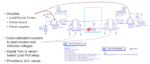
One of the most intriguing developments in recent years has been the emergence of Rapidus, a Japan-based foundry backed by government and major corporate investors. Rapidus aims to begin 2 nm class chip production around 2027, with plans to ramp monthly wafer production significantly within a year of launch.
From what I have learned about Rapidus over the last year, there is little doubt in my mind that they will succeed. In fact, Rapidus just raised another $1.7B for a total of $11.3B in combined government subsidies and private investment. While this is a significant sum, it represents about 40% of the $32 billion the company estimates it will need for full-scale mass production of 2-nanometer chips by 2027 so stay tuned.
Unlike the giants, Rapidus is not attempting to directly compete on sheer volume, but rather offering “short turnaround times” and tailored services, which could appeal to custom chip designers, domestic Japanese technology firms, and organizations needing smaller-lot, highly customized silicon.
Though still years behind TSMC in mass production timing and total capacity, Rapidus represents a strategic move by Japan to regain presence in advanced semiconductor manufacturing and create additional supply chain options in a market heavily concentrated among a few players.
The Broader Context: A Global Capacity Tightrope
The combined reality of TSMC’s dominant position, Intel’s internal and emerging foundry efforts, Samsung’s technically capable but constrained 2nm push, and the Rapidus niche entry creates a semiconductor landscape in which demand continues to outrun supply at the highest performance nodes. Even as worldwide fab capacity grows, the pace of AI adoption and the strategic value companies place on leading-edge silicon means securing wafer slots early has become mission-critical for tech giants and a formidable bottleneck for others.
Bottom line: The 2nm capacity crunch isn’t a short-term supply hiccup, it is a fundamental outcome of how advanced computing, AI, and custom silicon strategies are reshaping the global semiconductor ecosystem for years to come. The strength of the foundry business has always been based on mutil-sourcing and we need to get that supply chain strength back, absolutely.
Also Read:
TSMC Process Simplification for Advanced Nodes
TSMC and Cadence Strengthen Partnership to Enable Next-Generation AI and HPC Silicon