It has been an interesting month in the semiconductor business. Record revenues, profits, aggressive expansion plans, something we have not seen before and may not see again. Let’s start in Taiwan then move to Silicon Valley, Upstate New York, China, and Korea, with a look at: financials, capacity, and consolidation.
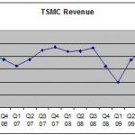
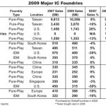
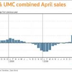
TSMC and UMC both posted record sales and profits exceeding even the optimistic. The top semiconductor companies followed suit which prompted the often quoted market researcher iSuppli to predict the chip industry is set for its highest annual growth in a decade: Semiconductor sales will climb to an all-time high of $300 billion in 2010, up from $230 billion last year. The previous sales record was $274 billion in 2007. According to iSupply, the last time semiconductor sales increased at such a rate was in 2000 when sales grew at 36.7%.
Though the semiconductor industry is estimated to grow 30%+ in 2010, TSMC and the foundry business is heading for much higher growth. Both fabless and fabbed semiconductor companies are reserving capacity with TSMC to ensure their SoCs hit the market window, compounding the wafer allocation problem that started earlier this year.
Capacity of course is key to semiconductor riches and will play the most significant role in who will deliver silicon to future generations. During my last visit to Taiwan, friends from TSMC briefed me on the Gigafab concept to which TSMC has publicly committed billions of dollars in capital expenses. A third $3B+ Gigafab will be constructed in the central Taiwanese city of Taichung and is slated to go online by the end of 2011. Nobody brings a new fab online faster and cheaper than TSMC, believe it.
While capitol spending is the key indicator of organic capacity growth, inorganic growth is also high on the foundry agenda: GlobalFoundry’s acquisition of Chartered Semiconductor, UMC’s investment in China’s He Jian, and TSMC’s equity stake in SMIC. GlobalFoundries clearly understands that capacity is everything in the foundry business, also understanding that they are no match for TSMC in a Fab building contest. Look for more inorganic growth for GlobalFoundries.
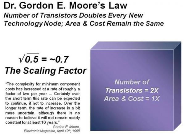
One of the leading semiconductor crystal ball sites predicted that there will only be three semiconductor manufacturers producing wafers below 20nm. It has been repeated so many times I don’t remember where it came from but now some view it as a truth. Today there are six foundries pushing Gordon Moore’s Empirical Observation: TSMC, UMC, GlobalFoundries, SMIC, Samsung, and IBM. That could certainly consolidate down to three: TSMC, Samsung, and GlobalFoundries.
While capitol spending is the key indicator of organic capacity growth, inorganic growth is also high on the foundry agenda: GlobalFoundry’s acquisition of Chartered Semiconductor, UMC’s investment in China’s He Jian, and TSMC’s equity stake in SMIC. GlobalFoundries clearly understands that capacity is everything in the foundry business, also understanding that they are no match for TSMC in a Fab building contest. Look for more inorganic growth for GlobalFoundries.
One of the leading semiconductor crystal ball sites predicted that there will only be three semiconductor manufacturers producing wafers below 20nm. It has been repeated so many times I don’t remember where it came from but now some view it as a truth. Today there are six foundries pushing Gordon Moore’s Empirical Observation: TSMC, UMC, GlobalFoundries, SMIC, Samsung, and IBM. That could certainly consolidate down to three: TSMC, Samsung, and GlobalFoundries.
lang: en_US